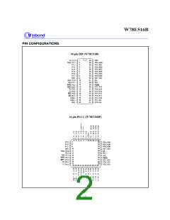
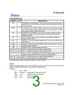
W78E516B
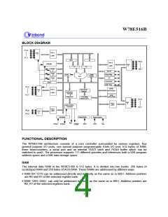
BLOCK DIAGRAM
P1.0
Port 1
Latch
Port
1
P1.7
ACC
B
P0.0
Port 0
Latch
Interrupt
Port
0
T1
T2
Timer
2
P0.7
DPTR
Timer
0
Stack
Pointer
Temp Reg.
PC
PSW
ALU
Timer
1
Incrementor
Addr. Reg.
UART
P3.0
P3.7
64KB
Port 3
Latch
SFR RAM
Address
Port
3
MTP-ROM
Instruction
Decoder
&
4KB
MTP-ROM
Sequencer
512 bytes
RAM & SFR
P2.0
Port
2
Port 2
Latch
Bus & Clock
Controller
P2.7
Port 4
Latch
P4.0
P4.3
Port
4
Oscillator
Reset Block
RST
Power control
ALE
XTAL1 XTAL2
VCC
Vss
PSEN
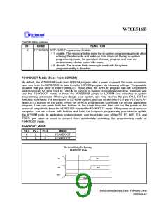
FUNCTIONAL DESCRIPTION
The W78E516B architecture consists of a core controller surrounded by various registers, four
general purpose I/O ports, one special purpose programmable 4-bits I/O port, 512 bytes of RAM,
three timer/counters, a serial port and an internal 74373 latch and 74244 buffer which can be
switched to port2. The processor supports 111 different opcodes and references both a 64K program
address space and a 64K data storage space.
RAM
The internal data RAM in the W78E516B is 512 bytes. It is divided into two banks: 256 bytes of
scratchpad RAM and 256 bytes of AUX-RAM. These RAMs are addressed by different ways.
·
-
RAM 0H 127H can be addressed directly and indirectly as the same as in 8051. Address pointers
are R0 and R1 of the selected register bank.
·
-
RAM 128H 255H can only be addressed indirectly as the same as in 8051. Address pointers are
R0, R1 of the selected registers bank.
- 4 -

 WINBOND [ WINBOND ]