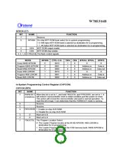
W78E516B
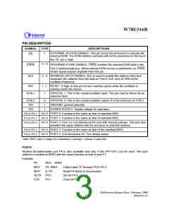
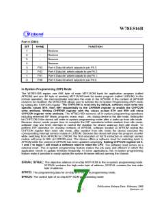
PIN DESCRIPTION
SYMBOL
TYPE
DESCRIPTIONS
I
EXTERNAL ACCESS ENABLE: This pin forces the processor to execute the
external ROM. The ROM address and data will not be presented on the bus if
EA
EA
the
pin is high.
O H
PSEN
ALE
PROGRAM STORE ENABLE: PSEN enables the external ROM data in the
PSEN
Port 0 address/data bus. When internal ROM access is performed, no
strobe signal outputs originate from this pin.
O H ADDRESS LATCH ENABLE: ALE is used to enable the address latch that
separates the address from the data on Port 0. ALE runs at 1/6th of the
oscillator frequency.
RST
I L RESET: A high on this pin for two machine cycles while the oscillator is
running resets the device.
XTAL1
XTAL2
I
CRYSTAL 1: This is the crystal oscillator input. This pin may be driven by an
external clock.
O
I
CRYSTAL 2: This is the crystal oscillator output. It is the inversion of XTAL1.
GROUND: ground potential.
SS
V
DD
V
I
POWER SUPPLY: Supply voltage for operation.
I/O D PORT 0: Function is the same as that of standard 8052.
I/O H PORT 1: Function is the same as that of standard 8052.
-
P0.0 P0.7
-
P1.0 P1.7
I/O H PORT 2: Port 2 is a bi-directional I/O port with internal pull-ups. This port also
provides the upper address bits for accesses to external memory.
-
P2.0 P2.7
I/O H PORT 3: Function is the same as that of the standard 8052.
I/O H PORT 4: A bi-directional I/O. See details below.
-
P3.0 P3.7
-
P4.0 P4.3
* Note:
I: input, O: output, I/O: bi-directional, H: pull-high, L: pull-low, D: open drain
TYPE
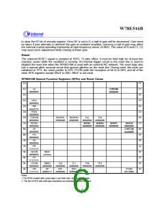
PORT4
Another bit-addressable port P4 is also available and only 4 bits (P4<3:0>) can be used. This port
address is located at 0D8H with the same function as that of port P1,
Example:
P4
REG 0D8H
P4, #0AH
A, P4
MOV
MOV
SETB
CLR
; Output data "A" through P4.0- P4.3.
; Read P4 status to Accumulator.
; Set bit P4.0
P4.0
P4.1
; Clear bit P4.1
Publication Release Date: February 2000
Revision A3
- 3 -

 WINBOND [ WINBOND ]