W78C32C/W78C032C
DC Characteristics, continued
SPECIFICATION
UNIT
PARAMETER
SYM.
TEST CONDITIONS
MIN.
TYP.
MAX.
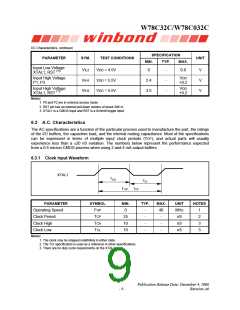
Input Low Voltage
XTAL1, RST (*3)
VIL2
VIH1
VIH2
VDD = 4.5V
VDD = 5.5V
VDD = 5.5V
0
-
0.8
V
V
V
Input High Voltage
P1, P3
VDD
+0.2
2.4
3.5
-
-
Input High Voltage
XTAL1, RST (*3)
VDD
+0.2
Notes:
1. P0 and P2 are in external access mode.
2. RST pin has an internal pull-down resistor of about 30K Ω.
3. XTAL1 is a CMOS input and RST is a Schmitt trigger input.
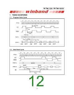
6.3 A.C. Characteristics
The AC specifications are a function of the particular process used to manufacture the part, the ratings
of the I/O buffers, the capacitive load, and the internal routing capacitance. Most of the specifications
can be expressed in terms of multiple input clock periods (TCP), and actual parts will usually
experience less than a ±20 nS variation. The numbers below represent the performance expected
from a 0.5 micron CMOS process when using 2 and 4 mA output buffers.
6.3.1 Clock Input Waveform
XTAL1
TCH
TCL
FOP,
TCP
PARAMETER
Operating Speed
Clock Period
SYMBOL
FOP
MIN.
0
TYP.
MAX.
UNIT
MHz
nS
NOTES
-
-
-
-
40
-
1
2
3
3
TCP
25
10
10
Clock High
TCH
-
nS
Clock Low
TCL
-
nS
Notes:
1. The clock may be stopped indefinitely in either state.
2. The TCP specification is used as a reference in other specifications.
3. There are no duty cycle requirements on the XTAL1 input.
Publication Release Date: December 4, 2006
Revision A6
- 9 -

 WINBOND [ WINBOND ]