W25Q16DV
Table of Contents
1.
2.
3.
GENERAL DESCRIPTION ...............................................................................................................5
FEATURES.......................................................................................................................................5
PACKAGE TYPES AND PIN CONFIGURATIONS...........................................................................6
3.1
3.2
3.3
3.4
3.5
3.6
3.7
3.8
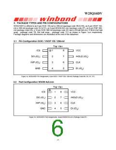
Pin Configuration SOIC / VSOP 150 / 208-mil .....................................................................6
Pad Configuration WSON 6x5-mm ......................................................................................6
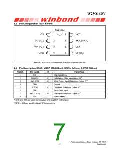
Pin Configuration PDIP 300-mil............................................................................................7
Pin Description SOIC / VSOP 150/208-mil, WSON 6x5-mm & PDIP 300-mil......................7
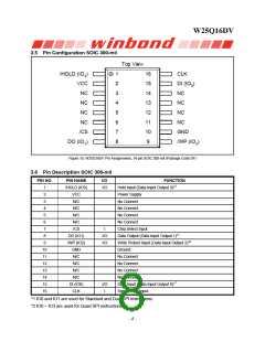
Pin Configuration SOIC 300-mil ...........................................................................................8
Pin Description SOIC 300-mil...............................................................................................8
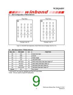
Ball Configuration TFBGA 8x6-mm ......................................................................................9
Ball Description TFBGA 8x6-mm .........................................................................................9
4.
PIN DESCRIPTIONS......................................................................................................................10
4.1
4.2
4.3
4.4
4.5
Chip Select (/CS)................................................................................................................10
Serial Data Input, Output and IOs (DI, DO and IO0, IO1, IO2, IO3)...................................10
Write Protect (/WP) ............................................................................................................10
HOLD (/HOLD) ...................................................................................................................10
Serial Clock (CLK)..............................................................................................................10
5.
6.
BLOCK DIAGRAM..........................................................................................................................11
FUNCTIONAL DESCRIPTION .......................................................................................................12
6.1
SPI OPERATIONS .............................................................................................................12
6.1.1 Standard SPI Instructions.....................................................................................................12
6.1.2 Dual SPI Instructions............................................................................................................12
6.1.3 Quad SPI Instructions...........................................................................................................12
6.1.4 Hold Function .......................................................................................................................12
6.2
WRITE PROTECTION .......................................................................................................13
6.2.1 Write Protect Features .........................................................................................................13
7.
STATUS REGISTERS AND INSTRUCTIONS ...............................................................................14
7.1
STATUS REGISTERS........................................................................................................14
7.1.1 BUSY Status (BUSY)............................................................................................................14
7.1.2 Write Enable Latch Status (WEL) ........................................................................................14
7.1.3 Block Protect Bits (BP2, BP1, BP0)......................................................................................14
7.1.4 Top/Bottom Block Protect Bit (TB)........................................................................................14
7.1.5 Sector/Block Protect Bit (SEC).............................................................................................14
7.1.6 Complement Protect Bit (CMP) ............................................................................................14
7.1.7 Status Register Protect Bits (SRP1, SRP0)..........................................................................15
7.1.8 Erase/Program Suspend Status (SUS) ................................................................................15
7.1.9 Security Register Lock Bits (LB3, LB2, LB1)........................................................................15
- 2 -

 WINBOND [ WINBOND ]