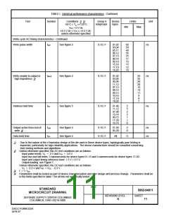
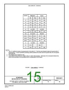
TABLE I. Electrical performance characteristics - Continued.
Test
Symbol
Conditions 1/ 2/
-55°C ≤ TC ≤+125°C
Group A
subgroups
Device
types
Limits
Unit
Min
Max
VSS = 0 V dc
+4.5 V dc ≤ VCC ≤ +5.5 V dc
unless otherwise specified
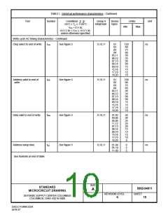
Write cycle AC timing characteristics - Continued.
Write pulse width
tWP
See figure 5
9,10,11
01,02
03,04
05,11
06,12
07,13
08,14
09,10
15,16
17,19
18,20
60
50
40
35
25
17
15
15
12
10
ns
Write enable to output in
high impedence 4/
tWHZ
See figure 5
9,10,11
01,02
03,04
05,06
11,12
07,13
08,14
09,15
10,16
17,19
18,20
35
25
20
20
15
13
11
9
ns
8
7
Address hold time
tAH
See figure 5
9,10,11
01-06
11,12
07,08
13,14
09,15
17-20
10,16
5
5
2
2
1
1
0
ns
Output active from end of
write 4/
tOW
See figure 5
See figure 5
9,10,11
9,10,11
01-04
05-20
5
0
ns
ns
Data hold time
tDH
All
0
1/
Due to the nature of the 4 transistor design of the die used in these device types, topologically pure testing is
important, particularly for high reliability applications. The device manufacturer should be consulted concerning
their testing methods and algorithms
2/ Unless otherwise specified, the AC test conditions are as follows:
Input pulse levels: VIL = 0 V and VIH = 3.0 V
Input rise and fall times: 5 nanoseconds for device types 01-16 and 3 nanoseconds for device types 17-20.
Input and output timing reference level: 1.5 V ± 0.5 V
Output loading: see Figure 7.
Unless otherwise specified, the DC test conditions are as follows:
VIL = 0.3 V and VIH = VCC - 0.3 V
3/ f = 1 / tAA
.
4/ Parameters shall be tested as part of device characterization and after design and process change. Parameters shall be
to the limits specified in table 1 for all lots not specifically tested.
SIZE
STANDARD
5962-94611
A
MICROCIRCUIT DRAWING
REVISION LEVEL
SHEET
DEFENSE SUPPLY CENTER COLUMBUS
COLUMBUS, OHIO 43216-5000
11
R
DSCC FORM 2234
APR 97

 WEDC [ WHITE ELECTRONIC DESIGNS CORPORATION ]