VITESSE
SEMICONDUCTOR CORPORATION
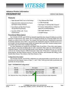
Advance Product Information
125MHz Octal Deskew
VSC6280/81/82
Operational Mode Truth Table
Mode No
Mode Name
TSTENN
CALENN
Mode Description
Measure vernier delays. Write data to data latches -
Transparent Mode. (Ring Oscillator Test)
1
Test Mode T
0
0
Measure vernier delay using latched data - Latched Mode.
(Ring Oscillator Test)
2
Test Mode L
0
1
Set timing delays with each vernier selected with ADR
[3:0] Serial Data Input.
3
4
Cal. Mode
User Mode
1
1
0
1
Generate timing delays as set by data in Cal Mode.
Figure 4: CAL Mode Timing Diagram
Odd Vernier Address
0001
Even Vernier Address
ADR[3:0]
0000
X X X
X X
∫∫
DCK
∫∫
11 Cycles
2 Cycles
CALENN
DIN
0
1
2
3
4
5
6
7
8
9
10
0
1
2
3
4
5
6
7
8
9 10
X X
X X X
X X
∫∫
LSP
MSP
LSB
MSB
TSTENN
Latch
Data
Latch Data
Load Calibration Register
Data Latch Transparent
Load Calibration Register
Data Latch Transparent
Measure Delay
1 CAL Cycle
Note:
TEST Mode Timing: Use CAL Mode Timing Diagram with TSTENN LO during CAL cycle. The TEST Mode places the verni-
ers in ring oscillator operation.
G52153-0, Rev. 2.2
8/5/98
VITESSE SEMICONDUCTOR CORPORATION
741 Calle Plano, Camarillo, CA 93012 • 805/388-3700 • FAX: 805/987-5896
Page 5

 VITESSE [ VITESSE SEMICONDUCTOR CORPORATION ]