VSC6134
Datasheet
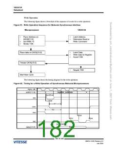
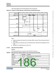
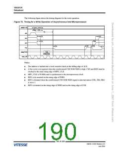
The following figure shows the timing diagram for the write operation.
Figure 66. Timing for a Write Operation of Synchronous Intel Microprocessor
mpu_clk
addr[11:0]
register_address
S0
adsn
D0
S1
csn
wrn
S2
D3
D1
D4
rdyrcvn
S3
data[15:0]
Data
Notes:
●
●
●
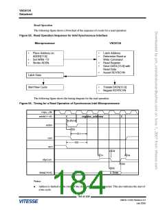
Address is latched on the rising of the clock when ADSN is asserted. This also indicates the start of
a bus cycle.
Data is latched on rising of the clock cycle following the one which detects the beginning of a bus
cycle.
RDYRCVN is asserted only for one clock cycle.
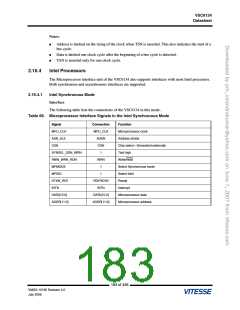
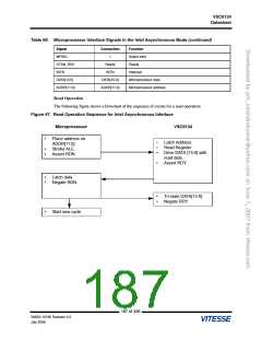
2.16.4.2
Intel Asynchronous Mode
Interface
The following table lists the connections of the VSC6134 in this mode.
Table 69. Microprocessor Interface Signals in the Intel Asynchronous Mode
Signal
Connection
MPU_CLK
ALE
Function
MPU_CLK
Microprocessor clock—Generated locally
Address strobe
ASN_ALE
CSN
CSN
Chip select—Generated externally
Write strobe
SYNSEL_DSN_WRN
RWN_WRN_RDN
MPMODE
WRN
RDN
Read strobe
0
Select Asynchronous mode
186 of 438
VMDS-10185 Revision 4.0
July 2006

 VITESSE [ VITESSE SEMICONDUCTOR CORPORATION ]