VSC6134
Datasheet
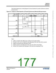
The following figure shows a timing diagram for the write operation for Motorola pseudo-synchronous
processors.
Figure 58. Timing for a Write Operation of Pseudo-Synchronous Motorola Microprocessors
mpu_clk
addr[11:0]
asn
register_address
S1
S0
S4
S2
D0
S3
csn
rwn
D6
D5
D2
D1
D4
dtkn
S5
data[15:0]
Data
Notes:
●
●
●
Address is latched on the falling edge of ASN into level-sensitive latches.
Data is latched on the rising edge of MPU_CLOCK following edge that detected a start of cycle.
The start of a bus cycle is recognized on the falling edge of the clock when ASN is asserted. The
VSC6134 determines that the bus cycle belongs to it if CSN is asserted at the beginning of the clock
edge following the edge that detected a start of cycle.
●
●
DTKN is de-asserted on the rising edge of ASN.
DTKN is tristated on the falling edge of the clock when ASN is detected high.
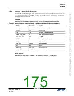
2.16.3.2
Motorola Synchronous Mode
In the Synchronous Interface mode, all signals (including the DTACKN) are expected to meet setup and
hold times of the processor clock. In Synchronous mode, the DTACKN is detected by the
microprocessor on the rising clock edge, and the data is also read in on the same edge.
179 of 438
VMDS-10185 Revision 4.0
July 2006

 VITESSE [ VITESSE SEMICONDUCTOR CORPORATION ]