S1A, S1B, S1D, S1G, S1J, S1K, S1M
www.vishay.com
Vishay General Semiconductor
ELECTRICAL CHARACTERISTICS (TA = 25 °C unless otherwise noted)
PARAMETER
TEST CONDITIONS
SYMBOL
S1A
S1B
S1D
S1G
S1J
S1K
S1M
UNIT
Maximum instantaneous
forward voltage
1.0 A
VF
1.1
V
TA = 25 °C
1.0
5.0
Maximum DC reverse current
IR
μA
at rated DC blocking voltage
TA = 125 °C
50
1.8
12
IF = 0.5 A, IR = 1.0 A,
Irr = 0.25 A
Typical reverse recovery time
Typical junction capacitance
trr
μs
4.0 V, 1 MHz
CJ
pF
THERMAL CHARACTERISTICS (TA = 25 °C unless otherwise noted)
PARAMETER
SYMBOL
S1A
S1B
S1D
75
S1G
S1J
S1K
S1M
UNIT
RJA
85
30
Typical thermal resistance (1)
°C/W
RJL
27
Note
(1)
Thermal resistance from junction to ambient and from junction to lead mounted on PCB with 0.2" x 0.2" (5.0 mm x 5.0 mm) copper pad areas
ORDERING INFORMATION (Example)
PREFERRED P/N
UNIT WEIGHT (g)
PREFERRED PACKAGE CODE
BASE QUANTITY
DELIVERY MODE
S1J-E3/61T
0.064
61T
5AT
61T
5AT
H
1800
7500
1800
7500
1800
7500
7" diameter plastic tape and reel
13" diameter plastic tape and reel
7" diameter plastic tape and reel
13" diameter plastic tape and reel
7" diameter plastic tape and reel
13" diameter plastic tape and reel
S1J-E3/5AT
0.064
S1JHE3/61T (1)
S1JHE3/5AT (1)
S1JHE3_A/H (1)
S1JHE3_A/I (1)
0.064
0.064
0.064
0.064
I
Note
(1)
AEC-Q101 qualified
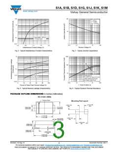
RATINGS AND CHARACTERISTICS CURVES (TA = 25 °C unless otherwise noted)
1.2
1.0
0.8
0.6
0.4
0.2
0
100
10
0
TL = 110 °C
8.3 ms Single Half Sine-Wave
Resistive or Inductive Load
S1A thru S1J
S1A thru S1J
S1K, S1M
S1K, S1M
0.2" x 0.2" (5.0 mm x 5.0 mm)
Thick Copper Pad Areas
1
10
100
0
20
40
60
80
100
120 140
160
Lead Temperature (°C)
Number of Cycles at 60 Hz
Fig. 1 - Forward Current Derating Curve
Fig. 2 - Maximum Non-Repetitive Peak Forward Surge Current
Revision: 19-Aug-13
Document Number: 88711
2
For technical questions within your region: DiodesAmericas@vishay.com, DiodesAsia@vishay.com, DiodesEurope@vishay.com
THIS DOCUMENT IS SUBJECT TO CHANGE WITHOUT NOTICE. THE PRODUCTS DESCRIBED HEREIN AND THIS DOCUMENT
ARE SUBJECT TO SPECIFIC DISCLAIMERS, SET FORTH AT www.vishay.com/doc?91000

 VISHAY [ VISHAY ]