IRFD020, SiHFD020
Vishay Siliconix
THERMAL RESISTANCE RATINGS
PARAMETER
SYMBOL
TYP.
MAX.
UNIT
Maximum Junction-to-Ambient
RthJA
-
120
°C/W
SPECIFICATIONS (TC = 25 °C, unless otherwise noted)
PARAMETER
SYMBOL
TEST CONDITIONS
MIN.
TYP.
MAX. UNIT
Static
Drain-Source Breakdown Voltage
Gate-Source Threshold Voltage
Gate-Source Leakage
VDS
VGS(th)
IGSS
VGS = 0 V, ID = 250 μA
VDS = VGS, ID = 250 μA
50
2.0
-
-
-
4.0
500
250
1000
-
V
V
-
VGS
VDS = max. rating, VGS = 0 V
VDS = max. rating x 0.8, VGS = 0 V, TC = 125
=
20 V
-
nA
-
-
-
Zero Gate Voltage Drain Current
IDSS
μA
-
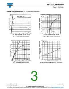
On-State Drain Currentb
Drain-Source On-State Resistanceb
Forward Transconductanceb
Dynamic
ID(on)
RDS(on)
gfs
VGS = 10 V
VGS = 10 V
VDS > ID(on) x RDS(on) max.
ID = 1.4 A
2.4
-
-
A
S
0.080
7.3
0.10
-
VDS = 20 V, ID = 7.5 A
4.9
Input Capacitance
Ciss
Coss
Crss
Qg
-
-
-
-
-
-
-
-
-
-
400
260
44
-
VGS = 0 V,
Output Capacitance
Reverse Transfer Capacitance
Total Gate Charge
VDS = 25 V,
-
pF
nC
f = 1.0 MHz
-
16
24
7.1
7.1
13
83
24
39
ID = 15 A,
DS = max. rating x 0.8
Gate-Source Charge
Gate-Drain Charge
Turn-On Delay Time
Rise Time
Qgs
Qgd
td(on)
tr
V
GS = 10 V
4.7
4.7
8.7
55
V
V
DD = 25 V, ID = 15 A,
Rg = 18 , RD = 1.7
ns
Turn-Off Delay Time
Fall Time
td(off)
tf
16
26
D
Between lead,
Internal Drain Inductance
LD
LS
-
-
4.0
6.0
-
-
6 mm (0.25") from
package and center of
die contact
nH
G
Internal Source Inductance
S
Drain-Source Body Diode Characteristics
Continuous Source-Drain Diode Current
MOSFET symbol
showing the
integral reverse
p - n junction diode
D
IS
-
-
-
-
2.4
19
A
G
Pulsed Diode Forward Currentc
ISM
S
Body Diode Voltagea
VSD
trr
TC = 25 °C, IS = 2.4 A, VGS = 0 V
TJ = 25 °C, IF = 15 A, dI/dt = 100 A/μs
-
-
1.4
310
0.85
V
Body Diode Reverse Recovery Time
Body Diode Reverse Recovery Charge
Forward Turn-On Time
57
130
0.34
ns
μC
Qrr
ton
0.17
Intrinsic turn-on time is negligible (turn-on is dominated by LS and LD)
Notes
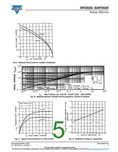
a. Repetitive rating; pulse width limited by maximum junction temperature (see fig. 11).
b. Pulse width 300 μs; duty cycle 2 %.
c. VDD = 25 V, starting TJ = 25 °C, L = 100 μH, Rg = 25
www.vishay.com
2
Document Number: 91465
S11-0915-Rev. A, 16-May-11
This document is subject to change without notice.
THE PRODUCTS DESCRIBED HEREIN AND THIS DOCUMENT ARE SUBJECT TO SPECIFIC DISCLAIMERS, SET FORTH AT www.vishay.com/doc?91000

 VISHAY [ VISHAY ]