IL420, IL4208
Vishay Semiconductors
Optocoupler, Phototriac Output,
High dV/dt, Low Input Current
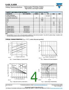
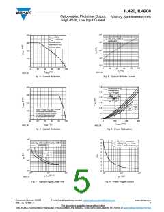
103
102
400
300
200
100
0
ITRMS = f(TA),
thJA = 150 K/W
Device switch
soldered in pcb
or base plate.
ID = f(Tj), VD = 600 V,
parameter:
R
Tj
101
100
10-1
0
20
40
60
80
100
0
20
40
60
80
100
Tj (°C)
iil420_08
Tamb (°C)
Fig. 5 - Current Reduction
iil420_05
Fig. 8 - Typical Off-State Current
0.6
0.5
400
300
200
100
0
for 40 Hz to 60 Hz
line operation,
P
= f(I
)
tot
TRMS
ITRMS
0.4
0.3
0.2
T
= 180 °C
= 120 °C
=
=
=
90 °C
60 °C
30 °C
I
= f(T
), R
PIN5
= 16.5 K/W
thJ-PIN5
TRMS
Thermocouple measurement must
be performed potentially separated
to A1 and A2. Measuring junction
as near as possible at the case.
0.1
0
0
100
200
300
50
60
70
80
90
100
ITRMS (mA)
TPIN5 (°C)
iil420_06
iil420_09
Fig. 6 - Current Reduction
Fig. 9 - Power Dissipation
103
10
9
I
= f (t ), I
pIF FTN
normalized
1.0 ms,
FTN
tgd = f(IF/IFT 25 °C),VD = 200V,
to I , referring to t
I ≥
FT pIF
= 200 V, f = 40 HZ to 60 Hz typ.
parameter:T
j
V
8
OP
7
102
6
Tj = 25 °C
100 °C
5
4
101
100
3
2
1
0
100
101
102
101
102
103
IF/IFT 25 °C
tpIF (µs)
iil420_07
Fig. 7 - Typical Trigger Delay Time
Fig. 10 - Pulse Trigger Current
Document Number: 83629
Rev. 2.0, 29-Mar-11
For technical questions, contact: optocoupleranswers@vishay.com
This document is subject to change without notice.
www.vishay.com
5
THE PRODUCTS DESCRIBED HEREIN AND THIS DOCUMENT ARE SUBJECT TO SPECIFIC DISCLAIMERS, SET FORTH AT www.vishay.com/doc?91000

 VISHAY [ VISHAY ]