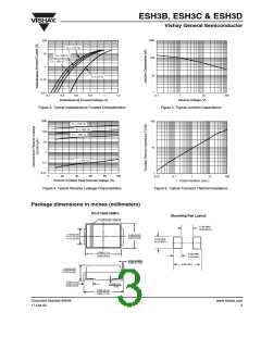
ESH3B, ESH3C & ESH3D
Vishay General Semiconductor
Electrical Characteristics
TA = 25 °C, unless otherwise specified
Parameter
Test condition
Symbo Value
l
Unit
at IF = 3 A(1)
Maximum instantaneous forward voltage
VF
0.90
V
Maximum DC reverse current at rated
DC blocking voltage
TA = 25 °C
IR
5.0
150
µA
TA = 125 °C
Maximum reverse recovery time
Typical reverse recovery time
at IF = 0.5 A, IR = 1 A, Irr = 0.25 A
trr
trr
25
ns
ns
at IF = 3 A, VR = 30 V di/dt = 50 A/µs, Irr = 10 % IRM TJ = 25 °C
TJ = 100 °C
40
55
Typical stored charge
at IF = 3 A, VR = 30 V di/dt = 50 A/µs, Irr = 10 % IRM TJ = 25 °C
TJ = 100 °C
Qrr
CJ
25
60
nC
pF
Typical junction capacitance
Note:
at 4.0 V, 1 MHz
70
(1) Pulse test: 300 µs pulse width, 1 % duty cycle
Thermal Characteristics
TA = 25 °C, unless otherwise specified
Parameter
Typical thermal resistance(1)
Symbol
RθJA
RθJL
ESH3B
ESH3C
ESH3D
Unit
°C/W
50
15
Note:
(1) Units mounted on P.C.B. with 12.0 x 12.0 mm land areas.
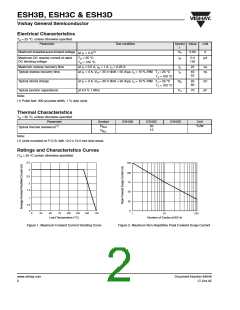
Ratings and Characteristics Curves
(TA = 25 °C unless otherwise specified)
3.5
3
125
100
75
2.5
2
1.5
50
1
25
0.5
0
0
1
0
25
50
75
100
125
150
175
10
Number of Cycles at 60 Hz
100
Lead Temperature (°C)
Figure 1. Maximum Forward Current Derating Curve
Figure 2. Maximum Non-Repetitive Peak Forward Surge Current
www.vishay.com
Document Number 84648
17-Oct-05
2

 VISHAY [ VISHAY ]