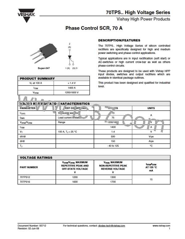
70TPS.. High Voltage Series
Phase Control SCR, 70 A
Vishay High Power Products
ABSOLUTE MAXIMUM RATINGS
PARAMETER
SYMBOL
TEST CONDITIONS
VALUES UNITS
Maximum average on-state current
IT(AV)
TC = 82 °C, 180° conduction half sine wave
70
Maximum continuous RMS on-state
current as AC switch
IT(RMS)
Lead current limitation
75
A
10 ms sine pulse, rated VRRM applied
10 ms sine pulse, no voltage reapplied
1200
1400
Maximum peak, one-cycle
non-repetitive surge current
ITSM
Initial TJ = TJ
maximum
10 ms sine pulse, rated VRRM applied
10 ms sine pulse, no voltage reapplied
t = 0.1 to 10 ms, no voltage reapplied
7200
A2s
Maximum I2t for fusing
I2t
10 200
Maximum I2√t for fusing
I2√t
VT(TO)1
VT(TO)2
rt1
102 000
0.916
1.21
4.138
3.43
1.4
A2√s
Low level value of threshold voltage
High level value of threshold voltage
Low level value of on-state slope resistance
High level value of on-state slope resistance
Maximum peak on-state voltage
Maximum rate of rise of turned-on current
Maximum holding current
V
TJ = 125 °C
mΩ
rt2
VTM
dI/dt
IH
100 A, TJ = 25 °C
TJ = 25 °C
V
150
A/µs
200
TJ = 25 °C
Maximum latching current
IL
400
mA
TJ = 25 °C
1.0
Maximum reverse and direct leakage current
Maximum rate of rise of off-state voltage
IRRM/IDRM
dV/dt
TJ = 125 °C
TJ = 125 °C
V
R = Rated VRRM/VDRM
15
500
V/µs
TRIGGERING
PARAMETER
SYMBOL
PGM
TEST CONDITIONS
VALUES UNITS
Maximum peak gate power
Maximum average gate power
Maximum peak gate current
Maximum peak negative gate voltage
10
W
2.5
T = 30 µs
PG(AV)
IGM
2.5
10
A
- VGM
TJ = - 40 °C
TJ = 25 °C
TJ = 125 °C
TJ = - 40 °C
TJ = 25 °C
TJ = 125 °C
4.0
1.5
1.1
270
100
80
V
Maximum required DC gate
voltage to trigger
VGT
Anode supply = 6 V resistive load
Maximum required DC gate current to trigger
IGT
mA
Maximum DC gate voltage not to trigger
Maximum DC gate current not to trigger
VGD
IGD
TJ = 120 °C, VDRM = Rated value
0.25
6
V
mA
www.vishay.com
2
For technical questions, contact: diodes-tech@vishay.com
Document Number: 93712
Revision: 02-Jun-08

 VISHAY [ VISHAY ]