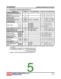
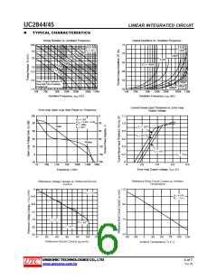
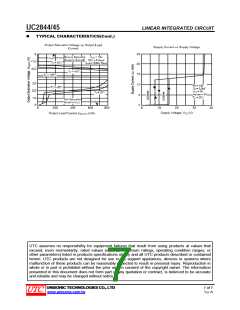
UC2844/45
LINEAR INTEGRATED CIRCUIT
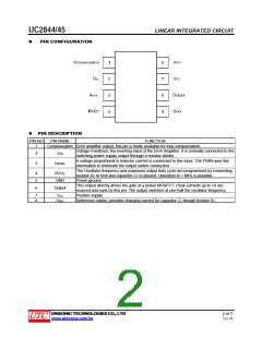
PIN CONFIGURATION
PIN DESCRIPTION
PIN NO
1
PIN NAME
FUNCTION
Compensation Error amplifier output, this pin is made available for loop compensation.
Voltage Feedback, the inverting input of the Error Amplifier. It is normally connected to the
switching power supply output through a resistor divider.
2
3
VFB
A voltage proportional to inductor current is connected to this input. The PWM uses this
information to terminate the output switch conduction.
ISENSE
The Oscillator frequency and maximum output duty cycle are programmed by connecting
resistor RT to Vref and capacitor CT to ground. Operation to 1 MHz is possible.
4
5
6
RT/CT
GND
Power ground.
This output directly drives the gate of a power MOSFET. Peak currents up to 1A are
sourced and sunk by this pin. The output switches at one-half the oscillator frequency.
Positive supply.
Output
7
8
VCC
VREF
Reference output, provides charging current for capacitor CT though resistor RT.
UNISONIC TECHNOLOGIES CO., LTD
2 of 7
Ver.A
www.unisonic.com.tw

 UTC [ Unisonic Technologies ]