Application Information
Application Information
Thermal Characteristics
The TS29151/52/53 series are high performance with
low dropout voltage regulator suitable for moderate to
high current and voltage regulator application. Its
350mA(typ) dropout voltage at full load and over
temperature makes it especially valuable in battery
power systems and as high efficiency noise filters in
post regulator applications. Unlike normal NPN
transistor design, where the base to emitter voltage
drop and collector to emitter saturation voltage limit the
minimum dropout voltage, dropout performance of the
PNP output of these devices is limited only by low Vce
saturation voltage.
TS29151/52/53 series linear regulators are simple to
use, the most complicated design parameters to
consider are thermal characteristics, thermal design
requires the following application specification
parameters:
Maximum ambient temperature, Ta
Output current, Iout
Output voltage, Vout
Input voltage, Vin
We calculate the power dissipation of the regulator
from these numbers and the device parameters from
this data sheet. A heatsink may be required depending
on the maximum power dissipation and maximum
ambient temperature of the application. Under all
possible operating conditions, the junction temperature
must be within the range specified under absolute
maximum ratings. To determine if the heatsink is
required, the power dissipated by the regulator, PD
must be calculated.
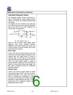
The TS29151/52/53 series is fully protected from
damage due to fault conditions. Linear current limiting is
provided. Output current during overload conditions is
constant. Thermal shutdown the device when the die
temperature exceeds the maximum safe operating
temperature. Transient protection allows device survival
even when the input voltage spikes above and below
nominal. The output structure of these regulators allows
voltages in excess of the desired output voltage to be
applied without reverse current flow.
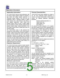
The below formula shows the voltages and currents for
calculating the PD in the regulator:
Iin = IL / IG
PD = (Vin-Vout) * IL + (Vin) * IG
Capacitor Requirement
Ex. PD = (3.3V-2.5V) * 0.5A + 3.3V * 11mA
= 400mW + 36mW
The TS29151/52/53 series requires an output capacitor
to maintain stability and improve transient response is
necessary. The value of this capacitor is dependent
upon the output current, lower currents allow smaller
capacitors. TS29151/52/53 series regulators are stable
with the 10uF minimum capacitor value at full load.
Where the regulator is powered from a source with high
AC impedance, a 0.1uF capacitor connected between
input and ground is recommended. The capacitor
should have good characteristics to above 250KHz. The
capacitance values will be help to improved transient
response, ripple rejection and output noise.
= 436mW
Remark: IL is output load current,
IG is ground current.
Vin is input voltage
Vout is output voltage
The next parameter which must be calculated is the
maximum allowable temperature rise, TR(max). this is
calculated by the using to formula:
TR(max) = TJ(max) – TA(max)
Where: TJ(max) is the maximum allowable junction
temperature, which is 125 oC for commercial
grade parts.
Minimum Load Current
TA(max)
is
the
maximum
ambient
The TS29151/52/53 series is specified between finite
loads. If the output current is too small leakage currents
dominate and the output voltage rises. A 10mA
minimum load current swamps any expected leakage
current across the operating temperature range.
temperature which will be encountered in the
application. Using the calculated values for TR(max)
and PD, the maximum allowable value for the junction
to ambient thermal resistance, θja, can now be found:
θja = TR(max) / PD
TS29151/52/53
5-5
2003/12 rev. D

 TSC [ TAIWAN SEMICONDUCTOR COMPANY, LTD ]