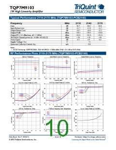
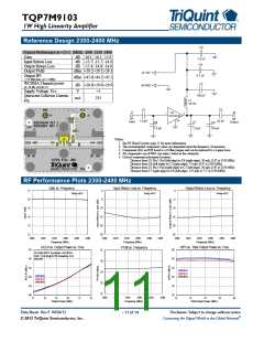
TQP7M9103
1W High Linearity Amplifier
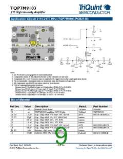
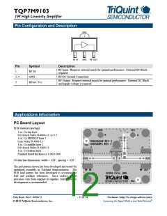
Pin Configuration and Description
GND
4
1
2
3
RF IN
GND
RF OUT
Pin
1
Symbol
RF IN
Description
RF Input. Requires external match for optimal performance. External DC Block
required.
2, 4
3
GND
RF/DC Ground Connection
RF Output. Requires external match for optimal performance. External DC Block
and supply voltage is required.
RFout / Vcc
Applications Information
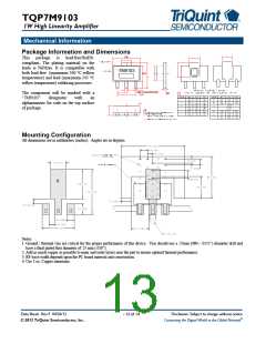
PC Board Layout
PCB Material (stackup):
1 oz. Cu top layer
0.014 inch Nelco N-4000-13, εr=3.7
1 oz. Cu MIDDLE layer 1
Core Nelco N-4000-13
1 oz. Cu middle layer 2
0.014 inch Nelco N-4000-13
1 oz. Cu bottom layer
Finished board thickness is 0.062±.006
50 ohm line dimensions: width = .028”, spacing = .028”.
The pad pattern shown has been developed and tested for
optimized assembly at TriQuint Semiconductor. The
PCB land pattern has been developed to accommodate
lead and package tolerances. Since surface mount
processes vary from supplier to supplier, careful process
development is recommended.
Data Sheet: Rev F 04/26/12
Disclaimer: Subject to change without notice
Connecting the Digital World to the Global Network®
- 12 of 14
© 2012 TriQuint Semiconductor, Inc.

 TRIQUINT [ TRIQUINT SEMICONDUCTOR ]