TQP7M9103
1W High Linearity Amplifier
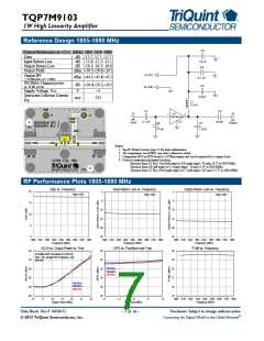
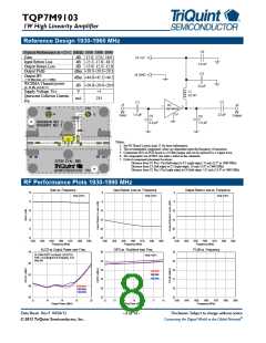
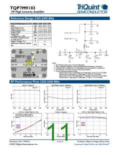
Reference Design 2300-2400 MHz
C5
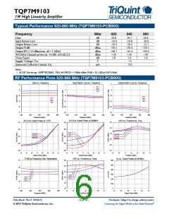
Typical Performance at +25 C (MHz) 2300 2350 2400
Gain
dB 16.1 16.1 15.9
dB -13.7 -15.7 -14.0
dB -15.4 -14.8 -14.0
dBm +29.2 +29.2 +29.3
1.0 uF
C4
Input Return Loss
Output Return Loss
Output P1dB
J3 +5V
0.1 uF
C3
Output IP3
dBm +45.6 +44.2 +45.2
dB +20.0 +19.9 +19.9
(+15 dBm/tone, ∆f = 1 MHz)
WCDMA Channel power
J4 GND
(at -50 dBc ACLR) [1]
Supply Voltage, Vcc
Quiescent Collector Current,
Icq
V
+5
100 pF
mA
235
L1
24 nH
C1
C2
J1
J2
U1
TQP7M9103
1
3
J4
J3
C5
C4
RF
Input
RF
Output
2,4
1.0 pF
22 pF
C7
C6
C8
1.0 pF
1.2 pF
0.6 pF
C3
U1
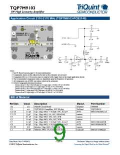
Notes:
1. See PC Board Layout, page 11 for more information.
2. The recommended component values are dependent upon the frequency of operation.
R1
C1
C2
3. Component (R1) on PCB board is a 0 Ohm jumper and can be replaced by a copper trace.
4. All components are of 0603 size unless stated on the schematic.
5. Critical component placement locations:
Distance from U1 Pin 1 Pad (left edge) to C6 (right edge): 30 mils (3.6º at 2350 MHz)
Distance from C6 (left edge) to C1 (right edge): 75 mils (8.9º at 2350 MHz)
Distance from U1 Pin 3 Pad (right edge) to C7 (left edge): 30 mils (3.6º at 2350 MHz)
Distance from C7 (right edge) to C8 (left edge): 147 mils (17.5º at 2350 MHz)
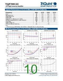
RF Performance Plots 2300-2400 MHz
Gain vs. Frequency
Input Return Loss vs. Frequency
Output Return Loss vs. Frequency
17
16
15
14
13
12
0
0
-5
Temp.=+25°C
Temp.=+25°C
Temp.=+25°C
-5
-10
-15
-20
-25
-10
-15
-20
-25
2300
2320
2340
2360
2380
2400
2300
2320
2340
2360
2380
2400
2300
2320
2340
2360
2380
2400
Frequency (MHz)
Frequency (MHz)
Frequency (MHz)
ACLR vs. Output Power vs. Freq
OIP3 vs. Total Output Power vs. Freq
P1dB vs. Frequency
-35
-40
-45
-50
-55
-60
50
45
40
35
30
25
31
30
29
28
27
W-CDMA 3GPP Test Model 1+64 DPCH,
PAR = 10.2 dB @ 0.01% Probability, 3.84
MHz BW
2300 MHz
2350 MHz
2400 MHz
2300 MHz
2350 MHz
2400 MHz
2300
2320
2340
2360
2380
2400
17
18
19
20
21
22
12
14
16
18
20
Output Power (dBm)
Frequency (MHz)
Total Output Power (dBm)
Data Sheet: Rev F 04/26/12
© 2012 TriQuint Semiconductor, Inc.
Disclaimer: Subject to change without notice
Connecting the Digital World to the Global Network®
- 11 of 14

 TRIQUINT [ TRIQUINT SEMICONDUCTOR ]