T E C H N I C A L I N F O R M A T I O N
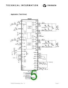
External Components Description (Refer to the Application/Test Circuit)
Components Description
RI
Inverting Input Resistance to provide AC gain in conjunction with RF. This input is biased at
the BIASCAP voltage (approximately 2.4VDC).
RF
Feedback resistor to set AC gain in conjunction with RI;
. Please refer to the
AV = 12(RF /RI)
Amplifier Gain paragraph in the Application Information section.
CI
AC input coupling capacitor which, in conjunction with RI, forms a highpass filter at
fC = 1 (2πRICI)
RREF
CA
Bias resistor. Locate close to pin 6 and ground at pin 8.
BIASCAP decoupling capacitor. Should be located close to pin 16.
Charge pump input capacitor. This capacitor should be connected directly between pins 2
and 3 and located physically close to the TA2024.
CD
CP
Charge pump output capacitor that enables efficient high side gate drive for the internal H-
bridges. To maximize performance, this capacitor should be connected directly between
pin 36 (CPUMP) and pin 34 (VDDA). Please observe the polarity shown in the Application/
Test Circuit.
CS
Supply decoupling for the low current power supply pins. For optimum performance, these
components should be located close to the pin and returned to their respective ground as
shown in the Application/Test Circuit.
CSW
Supply decoupling for the high current, high frequency H-Bridge supply pins. These
components must be located as close to the device as possible to minimize supply
overshoot and maximize device reliability. Both the high frequency bypassing (0.1uF) and
bulk capacitor (180uF) should have good high frequency performance including low ESR
and low ESL. Panasonic HFQ or FC capacitors are ideal for the bulk capacitor.
Zobel Capacitor.
CZ
RZ
Zobel resistor, which in conjunction with CZ, terminates the output filter at high frequencies.
The combination of RZ and CZ minimizes peaking of the output filter under both no load
conditions or with real world loads, including loudspeakers which usually exhibit a rising
impedance with frequency.
DO
LO
Schottky diodes that minimize undershoots of the outputs with respect to power ground
during switching transitions. For maximum effectiveness, these diodes must be located
close to the output pins and returned to their respective PGND. Please see
Application/Test Circuit for ground return pin.
Output inductor, which in conjunction with CO, demodulates (filters) the switching waveform
into an audio signal. Forms a second order filter with a cutoff frequency of
and a quality factor of
)
.
LO CO
fC = 1 (2π LO CO
Q = RL CO
CO
Output capacitor.
CCM
Common Mode Capacitor.
Page 6
TA2024 Preliminary, Rev. 1.0

 TRIPATH [ TRIPATH TECHNOLOGY INC. ]