TMC8462 Datasheet • Document Revision V1.4 • 2018-May -09
200 / 204
12 Figures Index
1
2
3
General device architecture . . . . . .
TMC8462 Evaluation Board . . . . . . 11
TMC8462 breakout board for RJ45 and
7
28 Status LED circuit . . . . . . . . . . . . 38
29 SII EEPROM circuit (shown for EEP-
ROMs >32kBit) . . . . . . . . . . . . . . 39
30 Direct PHY to PHY connection . . . . . 39
31 MFC IO Block Configuration using the
ESC Parameter RAM . . . . . . . . . . 111
32 MFC IO Crossbar Example Configuration151
33 MFC IO ESI/XML Configuration Block . 157
34 MFC IO Incremental Encoder Unit . . 158
35 Block structure of SPI Master Unit . . 160
36 Block structure of SPI Master Unit . . 165
37 Block structure of the MFC IO Step and
Direction Block . . . . . . . . . . . . . 169
38 Step & Direction Signal Timing . . . . 170
39 Block structure of the MFC IO PWM
Block . . . . . . . . . . . . . . . . . . . 172
40 PWM chopper modes . . . . . . . . . 174
41 PWM Timing (centered PWM) . . . . . 175
42 PWM Timing (left aligned PWM) . . . . 175
43 PWM Timing (right aligned PWM) . . . 176
44 PWM BBM Timing . . . . . . . . . . . . 176
45 Centered PWM with PWM channel 2
shifted from center (example showing
TPC . . . . . . . . . . . . . . . . . . . . 12
TMCL-IDE . . . . . . . . . . . . . . . . . 12
4
5
Configuration wizard example
MFC IO block configuration . . . . . . 13
Configuration wizard example
–
6
–
SII EEPROM content and C-code output 14
TMC8462-BA Pinout top view . . . . . 15
PDI control signals . . . . . . . . . . . 23
PDI SPI 2 byte addressing . . . . . . . 24
7
8
9
10 PDI SPI 3 byte addressing . . . . . . . 25
11 SPI timing example . . . . . . . . . . . 26
12 MFC control signals . . . . . . . . . . . 27
13 MFC CTRL SPI 2 byte addressing . . . 28
14 MFC CTRL SPI 3 byte addressing . . . 28
15 MFC SPI timing example . . . . . . . . 28
16 SPI bus sharing . . . . . . . . . . . . . 29
17 Physical bus interface pins . . . . . . . 30
18 Minimum external circuit for power-
on reset . . . . . . . . . . . . . . . . . . 31
19 PLL supply filter . . . . . . . . . . . . . 31
20 PHY power regulator filtering . . . . . 32
21 External circuit for switching regulator
0 with VS0 = 5V . . . . . . . . . . . . . 33
22 External circuit for switching regulator
0 with VS0 > 5V . . . . . . . . . . . . . 33
23 External circuit for adjustable buck
regulator . . . . . . . . . . . . . . . . . 34
24 Minimum external supply circuit for
single 3.3V supply . . . . . . . . . . . . 35
25 Minimum external supply circuit for
single 5V supply . . . . . . . . . . . . . 36
26 Minimum external supply circuit for
single supply >5V . . . . . . . . . . . . 37
27 Typical power supply chain using both
buck converters . . . . . . . . . . . . . 38
only 3 PWM channels) . . . . . . . . . 177
46 RC filter for DAC output with example
values . . . . . . . . . . . . . . . . . . . 178
47 Block structure of GPIO Unit . . . . . 179
48 Block structure of the MFC IO IRQ Block180
49 Logical position of the MFC IO watch-
dog unit between crossbar and MF-
CIOxx pins . . . . . . . . . . . . . . . . 181
50 Structure of the MFC IO watchdog unit 182
51 Schematic of multi voltage I/O port
. 186
52 Internal schematic and external com-
ponents for both switching regulators 188
53 TMC8462-BA package outline drawing 194
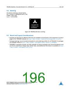
54 TMC8462-BA device marking . . . . . 196
©2018 TRINAMIC Motion Control GmbH & Co. KG, Hamburg, Germany
Terms of delivery and rights to technical change reserved.
Download newest version at www.trinamic.com

 TRINAMIC [ TRINAMIC MOTION CONTROL GMBH & CO. KG. ]