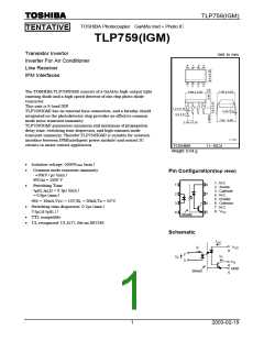
TLP759(IGM)
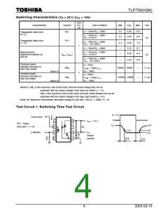
Switching Characteristics (Ta = 25°C,V = 15V)
CC
Test
Characteristic
Symbol
Cir-
Test Condition
= 10mA,R = 20kΩ
Min.
Typ.
Max.
Unit
µs
cuit
t
t
I
I
0.1
0.1
0.45
0.45
0.8
0.9
pHL
pLH
F
F
L
Propagation delay time
(H→L)
= 10mA,R = 20kΩ
L
Ta = 0~85°C
Propagation delay time
I
= 10mA,R = 20kΩ
L
F
(L→H)
0.1
―
0.45
0.15
0.25
1.0
0.7
0.8
Ta = -25~100°C
1
2
I
I
= 10mA,R = 20kΩ
L
F
F
Switching time
dispersion between on
and off
= 10mA,R = 20kΩ
L
―
|t
-t
|
µs
Ta = 0~85°C
pLH pHL
I
= 10mA,R = 20kΩ
L
F
―
0.25
0.9
Ta = -25~100°C
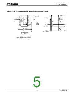
Common mode
I
V
= 0mA
F
transient immunity at
logic high output
CM
H
10000 15000
―
V / µs
V / µs
= 1500V
R = 20kΩ
=10mA
= 1500V
CM
L
p-p
p-p
(Note 9)
(Note 9)
Common mode
I
V
F
transient immunity at
logic low output
CM
L
-10000 -15000
―
CM
R = 20kΩ
L
(Note 9): CM is the maximum rate of fall of the common mode voltage that can be
L
sustained with the output voltage in the logic low state(V < 1V).
O
CM is the maximum rate of rise of the common mode voltage that can be
H
sustained with the output voltage in the logic high state(V < 4V).
O
(Note 10): Maximum electrostatic discharge voltage for any pins: 100V(C = 200pF, R = 0).
Test Circuit 1: Switching Time Test Circuit
I
F
0
I
F
Pulse input
1
2
3
4
8
7
6
5
V
V
= 15 V
CC
O
PW = 100µs
Duty ratio = 1 / 10
V
15V
O
R
L
1.5V
1.5V
I Monitor
F
V
OL
Output
monitor
t HL
p
t
pLH
4
2003-02-19

 TOSHIBA [ TOSHIBA ]