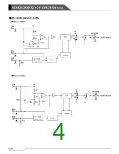
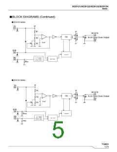
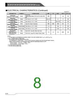
XC6121/XC6122/XC6123/XC6124 Series
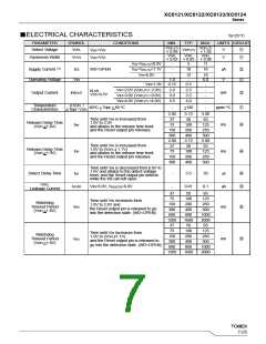
■ELECTRICAL CHARACTERISTICS (Continued)
Ta=25 OC
PARAMETER
SYMBOL
CONDITIONS
MIN.
TYP.
-
MAX.
-
UNITS CIRCUIT
VIN=6.0V,
Watchdog
Minimum Pulse Width
tWDIN
Apply pulse from 6.0V to 0V to the WD
pin.
300
ns
⑥
Watchdog
High Level Voltage
Watchdog
VWDH
VWDL
RWD
VIN=VDFL x 1.1V ~ 6.0V
VIN=VDFL x 1.1V ~ 6.0V
VWD=6V, RWD=VWD/IWD
VIN x 0.7
-
6
VIN x 0.3
900
V
V
⑥
⑥
⑦
⑧
⑧
0
300
1.3
0
-
Low Level Voltage
Watchdog
Pull-down Resistance
EN/ENB
600
kΩ
V
VENH/VENBH VIN=VDFL x 1.1V ~ 6.0V
VENL/VENBL VIN=VDFL x 1.1V ~ 6.0V
-
-
VIN
High Level Voltage
EN/ENB
0.35
V
Low Level Voltage
EN Pull-up
REN
VIN=6.0V, VEN=0V, REN=VIN / IEN
VIN=6.0V, VENB=6V, RENB=VENB / IENB
Resistance (*2)
ENB Pull-down
Resistance (*3)
1.0
1.6
2.4
MΩ
⑨
RENB
NOTE:
*
In case where no EN/ENB pin’s condition written in the test condition field, VEN=VIN and VENB=VSS
** VDFL(T)=Setting detect voltage value
(*1) The condition when the watchdog pin is ON.
.
The EN/ENB pin is CMOS input. For the XC6122 (pull-up resistor) and XC6124 (pull-down resistor),
supply current increases in the following values when the watchdog function is OFF.
XC6122 Series:(VIN-VEHL)/1.6MΩ(TYP.)
XC6124 Series:VEHBH/1.6MΩ(TYP.)
(*2) For the XC6122 series only.
(*3) For the XC6124 series only.
8/26

 TOREX [ Torex Semiconductor ]