XC6121/XC6122/XC6123/XC6124
Series
Ta=25 OC
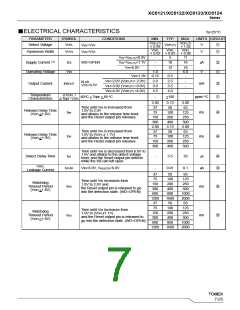
■ELECTRICAL CHARACTERISTICS
PARAMETER
SYMBOL
CONDITIONS
MIN.
TYP.
MAX.
UNITS CIRCUIT
VDFL(T)
× 0.98
VDFL
VDFL(T)
× 1.02
VDFL
Detect Voltage
VDFL
VDFL(T)
VDFL
V
V
①
①
V
EN=VSS
Hysteresis Width
VHYS
VEN=VSS
× 0.02 × 0.05 × 0.08
VIN=VDFL(T)×0.9V
-
5
11
Supply Current (*1)
Operating Voltage
ISS
VIN
WD=OPEN
VIN=VDFL(T)×1.1V
VIN=6.0V
-
10
16
μA
②
①
-
12
-
0.5
18
6.0
-
1.0
0.15
V
VIN=1.0V
VIN=2.0V (VDFL(T)> 2.0V)
VIN=3.0V (VDFL(T) >3.0V)
VIN=4.0V (VDFL(T) >4.0V)
O
2.0
3.0
3.5
2.5
3.5
4.0
-
-
-
N-ch.
VDS=0.5V
Output Current
IRBOUT
mA
③
①
Temperature
Characteristics
△VDFL /
O
O
△Topr・VDFL-40 C < Topr < 85 C
-
+100
-
ppm/ C
2.00
37
3.13
50
5.00
63
Time until VIN is increased from
Release Delay Time
(VDFL<1.8V)
1.0V to 2.0V
tDR
ms
④
④
75
100
200
400
3.13
50
125
250
500
5.00
63
and attains to the release time level,
and the Reset output pin releases.
150
300
2.00
37
Time until VIN is increased from
1.0V to (VDFL x 1.1V)
and attains to the release time level,
and the Reset output pin releases.
Release Delay Time
(VDFL>1.9V)
tDR
ms
75
100
200
400
125
250
500
150
300
Time until VIN is decreased from 6.0V to
1.0V and attains to the detect voltage
level, and the Reset output pin detects
while the WD pin left open.
Detect Delay Time
tDF
-
5.5
33
μs
④
③
VDFL
Leakage Current
ILEAK
VIN=6.0V, VRESETB=6.0V
-
0.01
0.1
μA
37
75
50
100
200
400
800
1600
50
63
125
250
500
1000
2000
63
Time until VIN increases form
1.0V to 2.0V and
the Reset output pin is released to go
into the detection state. (WD=OPEN)
Watchdog
Timeout Period
(VDFL<1.8V)
150
300
600
1200
37
tWD
ms
ms
⑤
⑤
75
100
200
400
800
1600
125
250
500
1000
2000
Time until VIN increases from
1.0V to (VDFLx1.1V)
and the Reset output pin is released to
go into the detection state. (WD=OPEN)
Watchdog
Timeout Period
(VDFL>1.9V)
150
300
600
1200
tWD
7/26

 TOREX [ Torex Semiconductor ]