ULN2002A, ULN2003A, ULN2003AI, ULN2004A
ULQ2003A, ULQ2004A
SLRS027J –DECEMBER 1976–REVISED JUNE 2010
www.ti.com
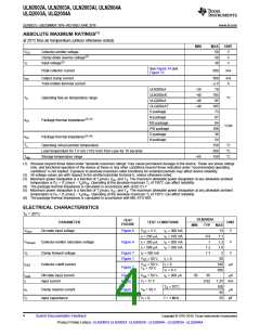
ABSOLUTE MAXIMUM RATINGS(1)
at 25°C free-air temperature (unless otherwise noted)
MIN
MAX
50
UNIT
VCC
Collector-emitter voltage
Clamp diode reverse voltage(2)
Input voltage(2)
V
V
V
50
VI
30
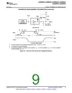
See Figure 14 and
Figure 15
Peak collector current
500
mA
IOK
Output clamp current
500
–2.5
70
mA
A
Total emitter-terminal current
ULN200xA
ULN200xAI
ULQ200xA
ULQ200xAT
D package
N package
NS package
PW package
D package
N package
–20
–40
–40
–40
105
85
TA
Operating free-air temperature range
°C
105
73
67
qJA
Package thermal impedance(3) (4)
Package thermal impedance(5) (6)
64
°C/W
108
36
qJC
54
TJ
Operating virtual junction temperature
150
260
150
°C
°C
°C
Lead temperature for 1.6 mm (1/16 inch) from case for 10 seconds
Storage temperature range
Tstg
–65
(1) Stresses beyond those listed under "absolute maximum ratings" may cause permanent damage to the device. These are stress ratings
only, and functional operation of the device at these or any other conditions beyond those indicated under "recommended operating
conditions" is not implied. Exposure to absolute-maximum-rated conditions for extended periods may affect device reliability.
(2) All voltage values are with respect to the emitter/substrate terminal E, unless otherwise noted.
(3) Maximum power dissipation is a function of TJ(max), qJA, and TA. The maximum allowable power dissipation at any allowable ambient
temperature is PD = (TJ(max) – TA)/qJA. Operating at the absolute maximum TJ of 150°C can affect reliability.
(4) The package thermal impedance is calculated in accordance with JESD 51-7.
(5) Maximum power dissipation is a function of TJ(max), qJC, and TA. The maximum allowable power dissipation at any allowable ambient
temperature is PD = (TJ(max) – TA)/qJC. Operating at the absolute maximum TJ of 150°C can affect reliability.
(6) The package thermal impedance is calculated in accordance with MIL-STD-883.
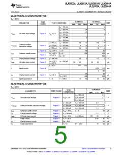
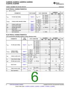
ELECTRICAL CHARACTERISTICS
TA = 25°C
ULN2002A
TEST
FIGURE
PARAMETER
On-state input voltage
TEST CONDITIONS
UNIT
MIN
TYP
MAX
13
VI(on)
VCE(sat)
VF
Figure 6
Figure 4
VCE = 2 V,
IC = 300 mA
IC = 100 mA
IC = 200 mA
IC = 350 mA
V
II = 250 mA,
II = 350 mA,
II = 500 mA,
IF = 350 mA
VCE = 50 V,
0.9
1
1.1
1.3
1.6
2
Collector-emitter saturation voltage
Clamp forward voltage
V
V
1.2
1.7
Figure 7
Figure 1
II = 0
50
ICEX
Collector cutoff current
VCE = 50 V,
TA = 70°C
II = 0
100
500
mA
mA
Figure 2
VI = 6 V
IC = 500 mA
II(off)
II
Off-state input current
Input current
Figure 2
Figure 3
VCE = 50 V,
VI = 17 V
50
65
0.82
1.25 mA
TA = 70°C
f = 1 MHz
100
mA
50
IR
Ci
Clamp reverse current
Input capacitance
Figure 6
VR = 50 V
VI = 0,
25
pF
4
Submit Documentation Feedback
Copyright © 1976–2010, Texas Instruments Incorporated
Product Folder Link(s): ULN2002A ULN2003A ULN2003AI ULN2004A ULQ2003A ULQ2004A

 TI [ TEXAS INSTRUMENTS ]