UCC1895
UCC2895
UCC3895
APPLICATION INFORMATION (CONT.)
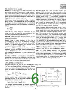
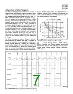
The Adaptive Delay Set feature (ADS) allows the user to ing the UC3879. Implementing this adaptive feature is
vary the delay times between switch commands within simplified in the UCC3895 controller, giving the user the
each of the converter’s two legs. The delay time modula- ability to tailor the delay times to suit a particular applica-
tion is implemented by connecting ADS (pin 11) to CS, tion with a minimum of external parts.
GND, or a resistive divider from CS to GND to set VADS
.
From the equation for VDEL above, if ADS is tied to GND
then VDEL rises in direct proportion to VCS, causing a de-
crease in tDELAY as the load increases. In this condition
the maximum value of VDEL is 2V. If ADS is connected to
a resistive divider between CS and GND the term
A = VADS/VCS RDELAY = 10kW
A=1.0
A=0.8
500
400
300
200
(VCS-VDS) becomes smaller, reducing the level of VDEL
.
This will decrease the amount of delay modulation. In the
limit of ADS tied to CS, VDEL=0.5V and no delay modula-
tion occurs. In the case with maximum delay modulation
(ADS=GND), when the circuit goes from light load to
heavy load the variation of VDEL is from 0.5V to 2V. This
causes the delay times to vary by a 4:1 ratio as the load
is changed.
A=0.6
A=0.4
A=0.2
A=0.1
100
0
0.5
1.0
1.5
2.0
2.5
CURRENT SENSE VOLTAGE (V)
The ability to program an adaptive delay is a desirable
feature because the optimum delay time is a function of
the current flowing in the primary winding of the trans-
former, and can change by a factor of 10:1 or more as
circuit loading changes. Reference [1] delves into the
many interrelated factors for choosing the optimum delay
times for the most efficient power conversion, and illus-
trates an external circuit to enable adaptive delay set us-
[1]
L. Balogh,
Unitrode Power
Supply Design Seminar Manual, Unitrode Corporation,
1996, Topic 2.
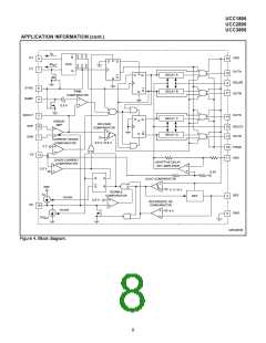
CLOCK
RAMP
&
COMP
PWM
SIGNAL
OUTPUT A
OUTPUT B
OUTPUT C
OUTPUT D
UDG-98138
7

 TI [ TEXAS INSTRUMENTS ]