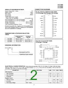
UCC1895
UCC2895
UCC3895
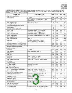
PIN DESCRIPTIONS (cont.)
After a fault or disable condition has
passed, VDD is above the start threshold, and/or
SS/DISB falls below 0.5V during a soft stop, SS/DISB will
switch to a soft start mode. The pin will now source
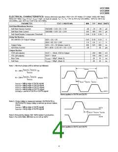
RAMP: The Inverting Input of the PWM Comparator. This
pin receives either the CT waveform in voltage and aver-
age current mode controls, or the current signal (plus
slope compensation) in peak current mode control. An in-
ternal discharge transistor is provided on RAMP, which is
triggered during the oscillator dead time.
current, equal to IRT
.
A user-selected capacitor on
SS/DISB determines the soft start (and soft-start) time. In
addition, a resistor in parallel with the capacitor may be
used, limiting the maximum voltage on SS/DISB. Note
that SS/DISB will actively clamp the EAOUT pin voltage
to approximately the SS/DISB pin voltage during both
soft start, soft stop, and disable conditions.
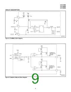
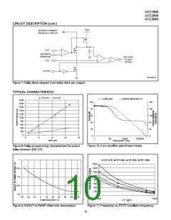
RT: Oscillator Timing Resistor. (Refer to Fig. 1, Oscillator
Block Diagram) The oscillator in the UCC3895 operates
by charging an external timing capacitor, CT, with a fixed
current programmed by RT. RT current is calculated as
follows:
SYNC: Oscillator Synchronization. (Refer to Fig. 1, Oscil-
lator Block Diagram) This pin is bidirectional. When used
as an output, SYNC can be used as a clock, which is the
same as the chip’s internal clock. When used as an in-
put, SYNC will override the chip’s internal oscillator and
act as it’s clock signal. This bidirectional feature allows
synchronization of multiple power supplies. The SYNC
signal will also internally discharge the CT capacitor and
any filter capacitors that are present on the RAMP pin.
The internal SYNC circuitry is level sensitive, with an in-
put low threshold of 1.9V, and an input high threshold of
2.1V. A resistor as small as 3.9kW may be tied between
SYNC and GND to reduce the sync pulse width.
3.0 V
IRT
=
RT
where RT is in Ohms and IRT is in Amperes. RT can
range from 40kW to 120kW Soft start charging and dis-
charging current are also programmed by IRT
.
SS/DISB: Soft Start/Disable. This pin combines the two
independent functions.
: A rapid shutdown of the chip is
accomplished by any one of the following: externally
forcing SS/DISB below 0.5V, externally forcing REF
below 4V, VDD dropping below the UNLO threshold, or an
overcurrent fault is sensed (CS = 2.5V).
VDD: Power Supply. VDD must be bypassed with a mini-
mum of a 1.0mF low ESR, low ESL capacitor to ground.
In the case of REF being pulled below 4V or an UVLO
condition, SS/DISB is actively pulled to ground via an
internal MOSFET switch. If an overcurrent is sensed,
SS/DISB will sink a current of (10 • IRT) until SS/DISB
falls below 0.5V.
REF: 5V, ±1.2% voltage reference. The reference
supplies power to internal circuitry, and can also supply
up to 5mA to external loads. The reference is shut down
during undervoltage lock-out but is operational during all
other disable modes. For best performance, bypass with
a 0.1mF low ESR, low ESL capacitor to ground.
Note that if SS/DISB is externally forced below 0.5V the
pin will start to source current equal to IRT. Also note that
the only time the part switches into the low IDD current
mode is when the part is in undervoltage lockout.
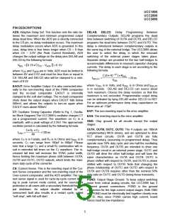
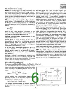
APPLICATION INFORMATION
Programming DELAB, DELCD, and the Adaptive Delay Set
The UCC3895 allows the user to set the delay between
switch commands within each leg of the full bridge power
circuit according to the following formula from the data
sheet:
UCC3895
CS 12
(25 • 10−12 )• RDEL
9
DELAB
tDELAY
=
+ 25nsec
VDEL
R
DELAB
10 DELCD
ADS 11
For this equation VDEL is determined in conjunction with
the desire to utilize (or not utilize) the adaptive delay set
feature from the following formula:
R
DELCD
(
)
VDEL =[0.75 • VCS − VADS ]+0.5V
The following diagram illustrates the resistors needed to
program the delay periods and the adaptive delay set
function.
6

 TI [ TEXAS INSTRUMENTS ]