UCC28180
www.ti.com
SLUSBQ5A –NOVEMBER 2013–REVISED NOVEMBER 2013
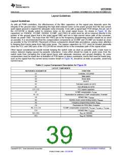
Layout Guidelines
Layout Guidelines
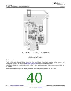
As with all PWM controllers, the effectiveness of the filter capacitors on the signal pins depends upon the
integrity of the ground return. Separating the high di/dt induced noise on the power ground from the low current
quiet signal ground is required for adequate noise immunity. Even with a signal layer PCB design, the pin out of
the UCC28180 is ideally suited to minimize noise on the small signal traces. As shown in Figure 36, the
capacitors on VSENSE, VCOMP, ISENSE, ICOMP, and FREQ (if used) must be all be returned directly to the
portion of the ground plane that is the quiet signal GND and not in high-current return path of the converter,
shown as power GND. The trace from the FREQ pin to the frequency programming resistor should be as short
as possible. It is recommended that the compensation components on ICOMP and VCOMP are located as close
as possible to the UCC28180. Placement of these components should take precedence, paying close attention
to keeping their traces away from high noise areas. The bypass capacitors on VCC must be located physically
close the VCC and GND pins of the UCC28180 but should not be in the immediate path of the signal return.
Other layout considerations should include keeping the switch node as short as possible, with a wide trace to
reduce induced ringing caused by parasitic inductance. Every effort should be made to avoid noise from the
switch node from corrupting the small signal traces with adequate clearance and ground shielding. As some
compromises must be made due to limitation of PCB layers or space constraints, traces that must be made long,
such as the signal from the current sense resistor shown in Figure 36, should be as wide as possible, avoid long
narrow traces.
Table 2. Layout Component Description for Figure 36
LAYOUT COMPONENTS
REFERENCE DESIGNATOR
FUNCTION
Controller, UCC28180
U1
Q1
Main switch
D2
Boost diode
R5
RGATE
R7
Pull-down resistor on GATE
Turn-off diode on GATE
D1
C11, C12
C7
VCC bypass capacitors
ICOMP compensation, CICOMP
Placeholders for additional ICOMP compensation, if needed
ISENSE filter, CISENSE
R1, C6
C8
R2
ISENSE inrush current limiting resistor, RISENSE
Frequency programming resistor, RFREQ
Placeholder for FREQ filter, if needed
VCOMP compensation components, RVCOMP, CVCOMP_P, CVCOMP
VSENSE filter, CVSENSE
R3
C9
R6, C13, C14
C15
R11, R12
R13
RFB1 on VSENSE
RFB2 on VSENSE
Copyright © 2013, Texas Instruments Incorporated
Submit Documentation Feedback
39
Product Folder Links :UCC28180

 TI [ TEXAS INSTRUMENTS ]