UCC27523, UCC27524, UCC27525, UCC27526
www.ti.com
SLUSAQ3E –NOVEMBER 2011–REVISED JUNE 2012
ELECTRICAL CHARACTERISTICS
VDD = 12 V, TA = TJ = -40°C to 140°C, 1-µF capacitor from VDD to GND. Currents are positive into, negative out of the
specified terminal (unless otherwise noted,)
PARAMETER
Bias Currents
TEST CONDITION
MIN
TYP
MAX
UNITS
VDD = 3.4 V,
INA=VDD,
INB=VDD
55
25
110
175
Startup current,
(based on UCC27524 Input
configuration)
IDD(off)
μA
VDD = 3.4 V,
INA=GND,
INB=GND
75
145
Under Voltage LockOut (UVLO)
TJ = 25°C
3.91
3.70
4.20
4.20
4.50
4.65
VON
Supply start threshold
TJ = -40°C to 140°C
V
Minimum operating voltage
after supply start
VOFF
3.40
0.20
3.90
0.30
4.40
0.50
VDD_H
Supply voltage hysteresis
Inputs (INA, INB, INA+, INA-, INB+, INB-), UCC2752X (D, DGN, DSD)
Output high for non-inverting input pins
Output low for inverting input pins
VIN_H
Input signal high threshold
1.9
2.1
2.3
Output low for non-inverting input pins
Output high for inverting input pins
V
V
VIN_L
Input signal low threshold
Input hysteresis
1.0
1.2
1.4
VIN_HYS
0.70
0.90
1.10
INPUTS (INA, INB, INA+, INA-, INB+, INB-) UCC27524P ONLY
Output high for non-inverting input pins
Output low for inverting input pins
VIN_H
Input signal high threshold
2.3
Output low for non-inverting input pins
Output high for inverting input pins
VIN_L
Input signal low threshold
Input hysteresis
1.0
VIN_HYS
0.9
Enable (ENA, ENB) UCC2752X (D, DGN, DSD)
VEN_H
VEN_L
Enable signal high threshold
Enable signal low threshold
Output enabled
Output disabled
1.9
0.95
0.70
2.1
1.15
0.95
2.3
1.35
1.10
V
V
VEN_HYS Enable hysteresis
ENABLE (ENA, ENB) UCC27524P ONLY
VEN_H
VEN_L
Enable signal high threshold
Enable signal low threshold
Output enabled
Output disabled
2.3
0.95
VEN_HYS Enable hysteresis
0.95
±5
Outputs (OUTA, OUTB)
ISNK/SRC Sink/source peak current(1)
VDD-VOH High output voltage
CLOAD = 0.22 µF, FSW = 1 kHz
IOUT = -10 mA
A
V
0.075
0.01
7.5
VOL
ROH
ROL
Low output voltage
Output pull-up resistance(2)
IOUT = 10 mA
IOUT = -10 mA
2.5
5
Ω
Ω
Output pull-down resistance
IOUT = 10 mA
0.15
0.5
1
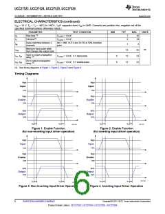
Switching Time
(1) Ensured by design.
(2) ROH represents on-resistance of only the P-Channel MOSFET device in pull-up structure of UCC2752X output stage.
Submit Documentation Feedback
Product Folder Link(s): UCC27523, UCC27524, UCC27525, UCC27526
Copyright © 2011–2012, Texas Instruments Incorporated
5

 TI [ TEXAS INSTRUMENTS ]