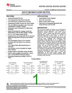
UCC27523, UCC27524, UCC27525, UCC27526
SLUSAQ3E –NOVEMBER 2011–REVISED JUNE 2012
www.ti.com
This integrated circuit can be damaged by ESD. Texas Instruments recommends that all integrated circuits be handled with
appropriate precautions. Failure to observe proper handling and installation procedures can cause damage.
ESD damage can range from subtle performance degradation to complete device failure. Precision integrated circuits may be more
susceptible to damage because very small parametric changes could cause the device not to meet its published specifications.
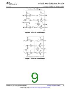
DESCRIPTION (CONT.)
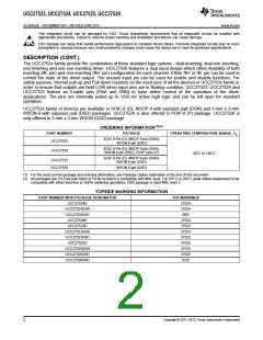
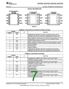
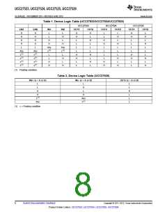
The UCC2752x family provide the combination of three standard logic options - dual-inverting, dual-non inverting,
one inverting and one non-inverting driver. UCC27526 features a dual input design which offers flexibility of both
inverting (IN- pin) and non-inverting (IN+ pin) configuration for each channel. Either IN+ or IN- pin can be used to
control the state of the driver output. The unused input pin can be used for enable and disable functions. For
safety purpose, internal pull-up and Pull-down resistors on the input pins of all the devices in UCC2752x family in
order to ensure that outputs are held LOW when input pins are in floating condition. UCC27323, UCC27324 and
UCC27325 feature an Enable pins (ENA and ENB) to have better control of the operation of the driver
applications. The pins are internally pulled up to VDD for active high logic and can be left open for standard
operation.
UCC2752x family of devices are available in SOIC-8 (D), MSOP-8 with exposed pad (DGN) and 3-mm x 3-mm
WSON-8 with exposed pad (DSD) packages. UCC27524 is also offered in PDIP-8 (P) package. UCC27526 is
only offered in 3-mm x 3-mm WSON (DSD) package.
ORDERING INFORMATION(1)(2)
PART NUMBER
PACKAGE
OPERATING TEMPERATURE RANGE, TA
SOIC 8-Pin (D), MSOP 8-pin (DGN),
WSON 8-pin (DSD)
UCC27523
SOIC 8-Pin (D), MSOP 8-pin (DGN),
WSON 8-pin (DSD), PDIP 8-pin (P)
UCC27524
-40°C to 140°C
SOIC 8-Pin (D), MSOP 8-pin (DGN),
WSON 8-pin (DSD)
UCC27525
UCC27526
WSON 8-pin (DSD)
(1) For the most current package and ordering information, see Package Option Addendum at the end of this document.
(2) All packages use Pb-Free lead finish of Pd-Ni-Au which is compatible with MSL level 1 at 255°C to 260°C peak reflow temperature to be
compatible with either lead free or Sn/Pb soldering operations. DSD package is rated MSL level 2.
TOPSIDE MARKING INFORMATION
PART NUMBER WITH PACKAGE DESIGNATOR
TOP MARKINGS
27524
UCC27524D
UCC27524DGN
27524
UCC27524DSD
SBA
UCC27524P
27524
UCC27523D
27523
UCC27523DGN
27523
UCC27523DSD
27523
UCC27525D
27525
UCC27525DGN
27525
UCC27525DSD
27525
UCC27526DSD
SCB
2
Copyright © 2011–2012, Texas Instruments Incorporated

 TI [ TEXAS INSTRUMENTS ]