ꢀ
ꢀ
ꢀ
ꢁ
ꢁ
ꢁ
ꢂ
ꢇ
ꢊ
ꢃ
ꢃ
ꢃ
ꢄ
ꢄ
ꢄ
ꢅ
ꢅ
ꢅ
ꢆ
ꢆ
ꢆ
ꢀꢁꢇ ꢃ ꢄ ꢅ ꢈꢉ
ꢀꢁꢊ ꢃ ꢄ ꢅ ꢈꢉ
SLUS329B − JUNE 1998 − REVISED FEBRUARY 2005
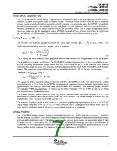
FUNCTIONAL DESCRIPTION
The UC3854A and UC3854B family of products are designed as pin compatible upgrades to the industry
standard UC3854 active power factor correction circuits. The circuit enhancements allow the user to eliminate
in most cases several external components currently required to successfully apply the UC3854. In addition,
linearity improvements to the multiply, square and divide circuitry optimizes overall system performance.
Detailed descriptions of the circuit enhancements are provided below. For in-depth design applications
reference data refer to the application notes, UC3854 Controlled Power Factor Correction Circuit Design
(SLUA144) and UC3854A and UC3854B Advanced Power Factor Correction Control ICs (SLUA177).
Multiply/Square and Divide
* 1
ǒ
Ǔ as the UC3854. The
The UC3854A/B multiplier design maintains the same gain constant K +
V
relationship between the inputs and output current is given as:
ǒV * 1.5 VǓ
VAO
I
+ I
MOUT
iAC
2
K ǒV
Ǔ
VRMS
(1)
This is nearly the same as the UC3854, but circuit differences have improved the performance and application.
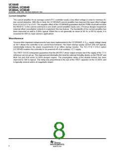
The first difference is with the IAC input. The UC3854A/B regulated this pin voltage to the nominal 500 mV over
the full operating temperature range, rather than the 6.0 V used on the UC3854. The low offset voltage
eliminates the need for a line zero crossing compensating resistor to VREF from IAC that UC3854 designs
require. The maximum current at high line into IAC should be limited to 250 µA for best performance.
Therefore, if V
= 270 V,
VAC(max)
270 1.414
250 mA
R
+
+ 1.53 MW
IAC
(2)
The V
pin linear operating range is improved with the UC3854A/B as well. The input range for VRMS
RMS
extends from 0 V to 5.5 V. Since the UC3854A squaring circuit employs an analog multiplier, rather than a linear
approximation, accuracy is improved, and discontinuities are eliminated. The external divider network
connected to VRMS should produce 1.5 V at low line (85 VAC). This puts 4.77 V on VRMS at high line (27 VAC)
which is well within its operating range.
The voltage amplifier output forms the third input to the multiplier and is internally clamped to 6.0 V. This
eliminated an external zener clamp often used in UC3854 designs. The offset voltage at this input to the
multiplier has been raised on the UC3854A/B to 1.5 V.
The multiplier output pin, which is also common to the current amplifier non-inverting input, has a −0.3 V to 5.0 V
output range, compared to the −0.3 V to 2.5 V range of the UC3854. This improvement allows the UC3854A/B
to be used in applications where the current sense signal amplitude is very large.
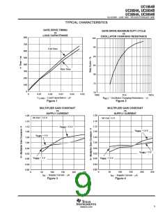
Voltage Amplifier
The UC3854A/B voltage amplifier design is essentially similar to the UC3854 with two exceptions. The first is
with the internal connection. The lower voltage reduces the amount of charge on the compensation capacitors,
which provides improved recovery form large signal events, such as line dropouts, or power interruption. It also
minimizes the dc current flowing through the feedback. The output of the voltage amplifier is also changes. In
addition to a 6.0 V temperature compensated clamp, the output short circuit current has been lowered to 2 mA
typical, and an active pull down has replaced the passive pull down of the UC3854.
7
www.ti.com

 TI [ TEXAS INSTRUMENTS ]