ꢀ
ꢀ
ꢀ
ꢁ
ꢁ
ꢁ
ꢂ
ꢇ
ꢊ
ꢃ
ꢃ
ꢃ
ꢄ
ꢄ
ꢄ
ꢅ
ꢅ
ꢅ
ꢆ
ꢆ
ꢆ
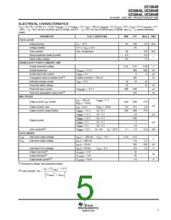
ꢀꢁꢇ ꢃ ꢄ ꢅ ꢈꢉ
ꢀꢁꢊ ꢃ ꢄ ꢅ ꢈꢉ
SLUS329B − JUNE 1998 − REVISED FEBRUARY 2005
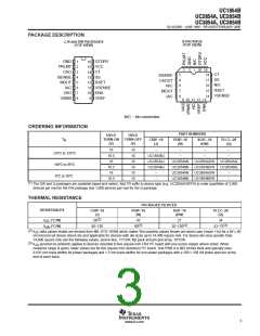
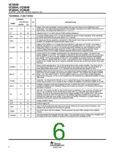
PACKAGE DESCRIPTION
Q PACKAGE
(TOP VIEW)
J, N and DW PACKAGES
(TOP VIEW)
GND
PKLMT
CAO
GTDRV
VCC
1
2
3
4
5
6
7
8
16
15
14
13
12
11
3
2
1
20 19
18
CT
CT
5
4
6
7
8
ISENSE
CAOUT
N/C
ISENSE
MOUT
IAC
SS
SS
17
16
15
14
RSET
VSENSE
N/C
RSET
VSENSE
MOUT
IAC
VAO
10 ENA
VREF
VRMS
9
9 10 11 12 13
N/C − No connection
ORDERING INFORMATION
PART NUMBERS
PDIP−16 SOIC−16
UVLO
TURN-ON
(V)
UVLO
TURN-OFF
(V)
T
A
CDIP−16
(J)
PLCC−20
(N)
(DW)
(Q)
16
10.5
16
10
10
10
10
10
10
−
−
−
−
−55°C to 125°C
−40°C to 85°C
0°C to 70°C
UC1854BJ
UC2854AJ
UC2854BJ
−
−
−
−
UC2854AN
UC2854BN
UC3854AN
UC3854BN
UC2854ADW
UC2854BDW
UC3854ADW
UC3854BDW
UC2854AQ
10.5
16
UC2854BQ
−
−
10.5
−
(1)
The DW and Q packages are available taped and reeled. Add TR suffix to device type (e.g. UC2854ADWTR) to order quantities of 2,000
devices per reel for the DW package and 1,000 devices per reel for the Q package.
THERMAL RESISTANCE
PACKAGED DEVICES
RESISTANCES
CDIP−16
(J)
PDIP−16
SOP−16
(DW)
PLCC−20
(Q)
(N)
(2)
28
θ
θ
(°C/W)
(°C/W)
45
27
34
JC
(3)
90
(3)
50−130
(3)
80−120
43−75
JA
(2)
(3)
θ
data values stated are derived from MIL-STD-1835B which states “the baseline values shown are worst case (mean +2s) for a 60 × 60
JC
mil microcircuit device silicon die and applicable for devices with die sizes up to 14,400 square mils. For device die sizes greater than
14,400 square mils use the following values, dual-in-line, 11°C/W; flat pack and pin grid array, 10°C/W.
θ
JA
(junction-to-ambient) applies to devices mounted to five square inch FR4 PC board with one ounce copper where noted. When
resitance range is given, lower values are for five square inch aluminum PC board. Test PWB is 0.062 inches thick and typically uses
0.635 mm trace widths for power packages and 1.3 mm trace widths for non-power packages with a 100 × 100 mil probe land are at the
end of each trace.
3
www.ti.com

 TI [ TEXAS INSTRUMENTS ]