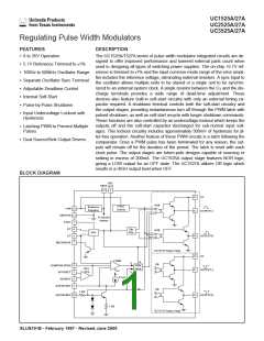
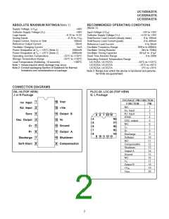
UC1525A/27A
UC2525A/27A
UC3525A/27A
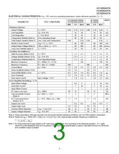
ELECTRICAL CHARACTERISTICS:+VIN = 20V, and over operating temperature, unless otherwise specified, TA = TJ.
UC1525A/UC2525A
UC1527A/UC2527A
UC3525A
UC3527A
UNITS
PARAMETER
Reference Section
TEST CONDITIONS
MIN
TYP
MAX
MIN
TYP
MAX
Output Voltage
TJ = 25°C
IN = 8 to 35V
5.05
5.10
10
5.15
20
5.00
5.10
10
5.20
20
V
Line Regulation
V
mV
mV
Load Regulation
IL = 0 to 20mA
20
50
20
50
Temperature Stability (Note 5)
Total Output Variation (Note 5)
Shorter Circuit Current
Output Noise Voltage (Note 5)
Long Term Stability (Note 5)
Oscillator Section(Note 6)
Initial Accuracy (Notes 5 & 6)
Voltage Stability (Notes 5 & 6)
Temperature Stability (Note 5)
Minimum Frequency
Over Operating Range
Line, Load, and Temperature
20
50
20
50
5.00
5.20
100
200
50
4.95
5.25
100
V
V
REF = 0, TJ = 25°C
80
40
20
80
40
20
mA
10Hz ≤ 10kHz, TJ = 25°C
200 µVrms
TJ = 125°C
50
mV
TJ = 25°C
± 2
± 0.3
± 3
± 6
± 1
± 6
120
± 2
± 1
± 3
± 6
± 2
± 6
120
%
%
VIN = 8 to 35V
Over Operating Range
RT = 200kΩ, CT = 0.1µF
RT = 2kΩ, CT = 470pF
%
Hz
kHz
mA
V
Maximum Frequency
400
1.7
3.0
0.3
1.2
400
1.7
3.0
0.3
1.2
Current Mirror
I
RT = 2mA
2.0
3.5
0.5
2.0
1.0
2.2
2.0
3.5
0.5
2.0
1.0
2.2
Clock Amplitude (Notes 5 & 6)
Clock Width (Notes 5 & 6)
Sync Threshold
TJ = 25°C
1.0
2.8
2.5
1.0
2.8
2.5
µs
V
Sync Input Current
Sync Voltage = 3.5V
mA
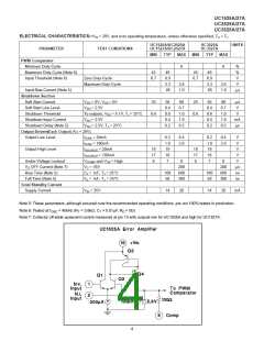
Error Amplifier Sectio(nVCM = 5.1V)
Input Offset Voltage
0.5
1
5
10
1
2
1
10
10
1
mV
µA
Input Bias Current
Input Offset Current
µA
DC Open Loop Gain
RL ≥ 10MΩ
60
1
75
2
60
1
75
2
dB
Gain-Bandwidth Product
(Note 5)
AV = 0dB, TJ = 25°C
MHz
DC Transconductance
(Notes 5 & 7)
TJ = 25°C, 30kΩ ≤ RL ≤ 1MΩ
1.1
1.5
1.1
1.5
mS
Output Low Level
0.2
5.6
75
0.5
0.2
5.6
75
0.5
V
V
Output High Level
3.8
60
50
3.8
60
50
Common Mode Rejection
Supply Voltage Rejection
V
V
CM = 1.5 to 5.2V
IN = 8 to 35V
dB
dB
60
60
Note 5: These parameters, although ensured over the recommended operating conditions, are not 100% tested in production.
Note 6: Tested at fOSC = 40kHz (RT = 3.6kW, CT = 0.01mF, RD = 0W). Approximate oscillator frequency is defined by:
1
f =
CT (0.7RT + 3RD )
Note 7: DC transconductance (gM) relates to DC open-loop voltage gain (AV) according to the following equation: AV = gMRL
where RL is the resistance from pin 9 to ground. The minimum gM specification is used to calculate minimum AV when the
error amplifier output is loaded.
3

 TI [ TEXAS INSTRUMENTS ]