TXB0302
www.ti.com
SCES837A –MARCH 2012–REVISED MAY 2012
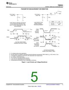
PARAMETER MEASUREMENT INFORMATION
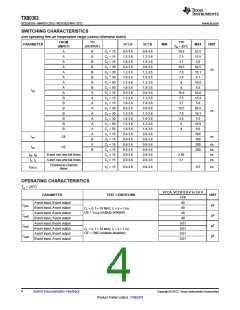
2 × V
CCO
S1
50 k
Open
From Output
Under Test
From Output
Under Test
CL
50 k
CL
50 k
TEST
/t
S1
2 × V
LOAD CIRCUIT FOR
ENABLE/DISABLE
TIME MEASUREMENT
LOAD CIRCUIT FOR MAX DATA RATE,
PULSE DURATION PROPAGATION
DELAY OUTPUT RISE AND FALL TIME
MEASUREMENT
t
PZL PLZ
CCO
t
/t
PHZ PZH
Open
V
CCA
Output
Control
V
CCI
Input
V
CCI
/2
V
CCI
/2
V
CCA
/2
V
CCA
/2
(low-level
enabling)
0 V
0 V
t
t
PLH
PHL
t
PLZ
t
V
OH
PZL
0.9
0.1
V
CCO
V
V
Output
CCO
V
/2
V
/2
Output
CCO
CCO
V
/2
V
CCO
CCO
Waveform 1
V
OL
V
0.1
0.9
CCO
t
f
t
r
S1 at 2 × V
CCO
OL
(see Note B)
t
PHZ
t
VOLTAGE WAVEFORMS
PROPAGATION DELAY TIMES
PZH
Output
Waveform 2
S1 at GND
V
OH
V
CCO
V
CCO
/2
(see Note B)
0 V
VOLTAGE WAVEFORMS
ENABLE AND DISABLE TIMES
A. C includes probe and jig capacitance.
L
B. All input pulses are supplied by generators having the following characteristics: PRR 10 MHz, Z = 50 Ω, dv/dt ≥ 1 V/ns.
O
C. The outputs are measured one at a time, with one transition per measurement.
D.
E.
F.
t
and t
are the same as t .
PLH
PHL pd
V
V
is the V associated with the input port.
CC
CCI
is the V associated with the output port.
CC
CCO
G. All parameters and waveforms are not applicable to all devices.
Figure 1. Load Circuits and Voltage Waveforms
Copyright © 2012, Texas Instruments Incorporated
Submit Documentation Feedback
5
Product Folder Link(s) :TXB0302

 TI [ TEXAS INSTRUMENTS ]