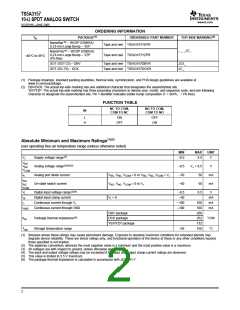
TS5A3157
10-Ω SPDT ANALOG SWITCH
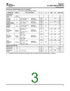
www.ti.com
SCDS199–JUNE 2005
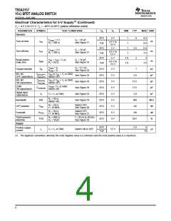
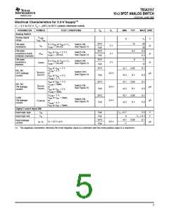
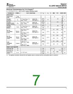
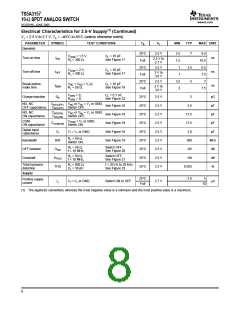
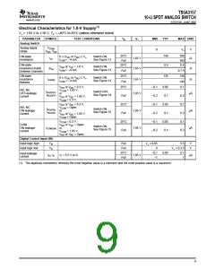
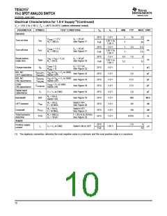
Electrical Characteristics for 3.3-V Supply(1) (Continued)
V+ = 3 V to 3.6 V, TA = –40°C to 85°C (unless otherwise noted)
PARAMETER
Dynamic
SYMBOL
TEST CONDITIONS
TA
V+
MIN
TYP
MAX UNIT
25°C
Full
3.3 V
3.5
1.5
1
7
9.5
VCOM = 2 V,
RL = 300 Ω,
CL = 35 pF,
See Figure 17
Turn-on time
Turn-off time
tON
ns
3 V to
3.6 V
10.5
25°C
Full
3.3 V
3.5
3
6.5
VCOM = 2 V,
RL = 300 Ω,
CL = 35 pF,
See Figure 17
tOFF
ns
3 V to
3.6 V
1
7.5
25°C
Full
3.3 V
2.5
2
5
Break-before-
make time
VNC = VNO = V+/2,
RL = 50 Ω,
CL = 35 pF,
See Figure 18
tBBM
ns
5
3 V to
3.6 V
VGEN = 0,
RGEN = 0,
CL = 0.1 nF,
See Figure 22
Charge injection
QC
CNO(OFF)
25°C
25°C
25°C
25°C
25°C
25°C
25°C
25°C
25°C
3.3 V
3.3 V
3.3 V
3.3 V
3.3 V
3.3 V
3.3 V
3.3 V
3.3 V
3
5.5
pC
pF
NO, NC
OFF capacitance
,
VNO or VNc = V+ or GND,
CNC(OFF) Switch OFF,
See Figure 16
See Figure 16
See Figure 16
See Figure 16
See Figure 19
NO, NC
ON capacitance
CNO(ON)
,
VNO or VNc = V+ or GND,
Switch OFF,
17.5
17.5
2.8
pF
CNC(ON)
COM
ON capacitance
VCOM = V+ or GND,
Switch ON,
CCOM(ON)
pF
Digital input
capacitance
CI
VI = V+ or GND,
pF
RL = 50 Ω,
Switch ON,
Bandwidth
OFF isolation
Crosstalk
BW
300
MHz
dB
dB
%
RL = 50 Ω,
f = 10 MHz,
Switch OFF,
See Figure 20
OISO
XTALK
THD
–65
RL = 50 Ω,
f = 10 MHz,
Switch OFF,
See Figure 21
–66
Total harmonic
distortion
RL = 600 Ω,
CL = 50 pF,
f = 20 Hz to 20 kHz,
See Figure 23
0.015
Supply
25°C
2.5
5
µA
10
Positive supply
current
I+
VI = V+ or GND,
Switch ON or OFF
3.3 V
Full
(1) The algebraic convention, whereby the most negative value is a minimum and the most positive value is a maximum.
6

 TI [ TEXAS INSTRUMENTS ]