TS5A3157
10-Ω SPDT ANALOG SWITCH
www.ti.com
SCDS199–JUNE 2005
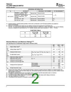
ORDERING INFORMATION
TA
PACKAGE(1)
ORDERABLE PART NUMBER
TOP-SIDE MARKING(2)
NanoStar™ – WCSP (DSBGA)
0.23-mm Large Bump – YEP
Tape and reel TS5A3157YEPR
_ _ _JC_
NanoFree™ – WCSP (DSBGA)
0.23-mm Large Bump – YZP
(Pb-free)
Tape and reel TS5A3157YZPR
–40°C to 85°C
SOT (SOT-23) – DBV
SOT (SC-70) – DCK
Tape and reel TS5A3157DBVR
Tape and reel TS5A3157DCKR
JC5_
JC_
(1) Package drawings, standard packing quantities, thermal data, symbolization, and PCB design guidelines are available at
www.ti.com/sc/package.
(2) DBV/DCK: The actual top-side marking has one additional character that designates the assembly/test site.
YEP/YZP: The actual top-side marking has three preceding characters to denote year, month, and sequence code, and one following
character to designate the assembly/test site. Pin 1 identifier indicates solder-bump composition (1 = SnPb, = Pb-free).
FUNCTION TABLE
NC TO COM,
COM TO NC
NO TO COM,
COM TO NO
IN
L
ON
OFF
ON
H
OFF
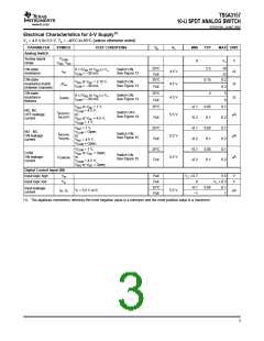
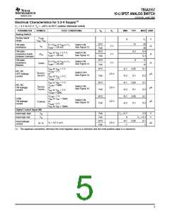
Absolute Minimum and Maximum Ratings(1)(2)
over operating free-air temperature range (unless otherwise noted)
MIN
MAX
UNIT
V+
Supply voltage range(3)
Analog voltage range(3)(4)(5)
Analog port diode current
On-state switch current
–0.5
6.5
V
VNO
VNC
VCOM
–0.5
–50
–50
V+ + 0.5
50
V
IK
VNC, VNO, VCOM < 0 or VNO, VNC, VCOM > V+
VNC, VNO, VCOM = 0 to V+
mA
mA
INO
INC
50
ICOM
VI
Digital input voltage range(3)(4)
Digital input clamp current
–0.5
–50
6.5
V
IIK
VI < 0
mA
mA
mA
I+
Continuous current through V+
Continuous current through GND
–100
–100
100
100
206
252
132
150
IGND
DBV package
θJA
Package thermal impedance(6)
DCK package
°C/W
°C
YEP/YZP package
Tstg
Storage temperature range
–65
(1) Stresses above these ratings may cause permanent damage. Exposure to absolute maximum conditions for extended periods may
degrade device reliability. These are stress ratings only, and functional operation of the device at these or any other conditions beyond
those specified is not implied.
(2) The algebraic convention, whereby the most negative value is a minimum and the most positive value is a maximum.
(3) All voltages are with respect to ground, unless otherwise specified.
(4) The input and output voltage ratings may be exceeded if the input and output clamp-current ratings are observed.
(5) This value is limited to 5.5 V maximum.
(6) The package thermal impedance is calculated in accordance with JESD 51-7.
2

 TI [ TEXAS INSTRUMENTS ]