TS3USB221A-Q1
www.ti.com
SCDS300B –JULY 2010–REVISED JULY 2011
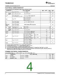
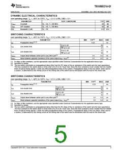
DYNAMIC ELECTRICAL CHARACTERISTICS
over operating range, TA = –40°C to 125°C, VCC = 2.5 V ±10%, GND = 0 V
PARAMETER
Crosstalk
TEST CONDITIONS
TYP UNIT
XTALK
OIRR
BW
RL = 50 , f = 250 MHz
RL = 50 , f = 250 MHz
RL = 50
-39
-40
0.9
dB
dB
OFF isolation
Bandwidth (3 dB)
GHz
SWITCHING CHARACTERISTICS
over operating range, TA = –40°C to 125°C, VCC = 3.3 V ±10%, GND = 0 V
PARAMETER
MIN
TYP(1)
MAX
UNIT
tpd
Propagation delay(2) (3)
Line enable time
0.25
ns
S to D, nD
OE to D, nD
S to D, nD
OE to D, nD
30
17
tON
ns
ns
12
tOFF
Line disable time
10
tSK(O)
tSK(P)
Output skew between center port to any other port(2)
0.1
0.1
0.2
0.2
ns
ns
(2)
Skew between opposite transitions of the same output (tPHL– tPLH
)
(1) For Max or Min conditions, use the appropriate value specified under Electrical Characteristics for the applicable device type.
(2) Specified by design
(3) The bus switch contributes no propagational delay other than the RC delay of the on resistance of the switch and the load capacitance.
The time constant for the switch alone is of the order of 0.25 ns for 10-pF load. Since this time constant is much smaller than the rise/fall
times of typical driving signals, it adds very little propagational delay to the system. Propagational delay of the bus switch, when used in
a system, is determined by the driving circuit on the driving side of the switch and its interactions with the load on the driven side.
SWITCHING CHARACTERISTICS
over operating range, TA = –40°C to 125°C, VCC = 2.5 V ±10%, GND = 0 V
PARAMETER
MIN TYP(1)
MAX
UNIT
tpd
Propagation delay(2) (3)
Line enable time
0.25
ns
S to D, nD
OE to D, nD
S to D, nD
OE to D, nD
50
32
tON
ns
ns
23
tOFF
Line disable time
12
tSK(O)
tSK(P)
Output skew between center port to any other port(2)
0.1
0.1
0.2
0.2
ns
ns
(2)
Skew between opposite transitions of the same output (tPHL– tPLH
)
(1) For Max or Min conditions, use the appropriate value specified under Electrical Characteristics for the applicable device type.
(2) Specified by design
(3) The bus switch contributes no propagational delay other than the RC delay of the on resistance of the switch and the load capacitance.
The time constant for the switch alone is of the order of 0.25 ns for 10-pF load. Since this time constant is much smaller than the rise/fall
times of typical driving signals, it adds very little propagational delay to the system. Propagational delay of the bus switch, when used in
a system, is determined by the driving circuit on the driving side of the switch and its interactions with the load on the driven side.
Copyright © 2010–2011, Texas Instruments Incorporated
5

 TI [ TEXAS INSTRUMENTS ]