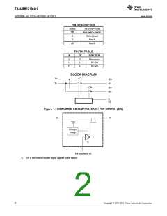
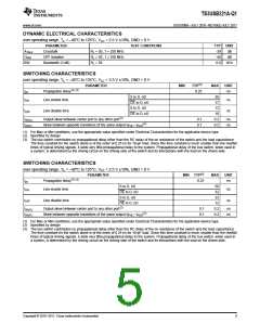
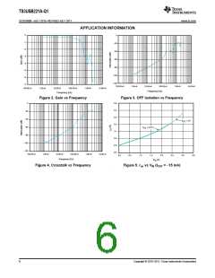
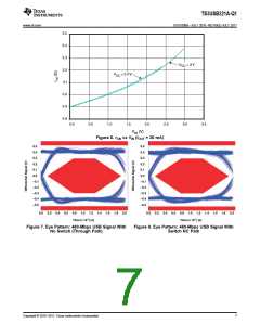
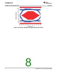
TS3USB221A-Q1
www.ti.com
SCDS300B –JULY 2010–REVISED JULY 2011
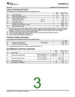
ABSOLUTE MAXIMUM RATINGS(1)
over operating free-air temperature range (unless otherwise noted)
MIN
–0.5
–0.5
–0.5
MAX
4.6
UNIT
V
VCC
VIN
VI/O
IIK
Supply voltage range
Control input voltage range(2) (3)
Switch I/O voltage range(2) (3) (4)
Control input clamp current
I/O port clamp current
7
V
7
V
V
IN < 0
–50
–50
±120
±100
150
mA
mA
mA
mA
°C
II/OK
II/O
VI/O < 0
ON-state switch current(5)
Continuous current through VCC or GND
Storage temperature range
Tstg
–65
(1) Stresses beyond those listed under "absolute maximum ratings" may cause permanent damage to the device. These are stress ratings
only, and functional operation of the device at these or any other conditions beyond those indicated under "recommended operating
conditions" is not implied. Exposure to absolute-maximum-rated conditions for extended periods may affect device reliability.
(2) All voltages are with respect to ground, unless otherwise specified.
(3) The input and output voltage ratings may be exceeded if the input and output clamp-current ratings are observed.
(4) VI and VO are used to denote specific conditions for VI/O
.
(5) II and IO are used to denote specific conditions for II/O
.
PACKAGE THERMAL IMPEDANCE
over operating free-air temperature range (unless otherwise noted)
UNIT
°C/W
°C/W
θJA
θJC
Package thermal impedance(1)
RSE package
243
84
Junction-to-case thermal resistance
(1) The package thermal impedance is calculated in accordance with JESD 51-7.
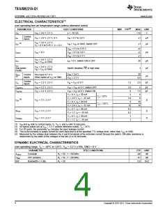
RECOMMENDED OPERATING CONDITIONS
MIN
2.3
MAX
UNIT
VCC
VIH
Supply voltage
3.6
V
VCC = 2.3 V to 2.7 V
VCC = 2.7 V to 3.6 V
VCC = 2.3 V to 2.7 V
VCC = 2.7 V to 3.6 V
0.46 × VCC
0.46 × VCC
High-level control input voltage
V
V
0.25 × VCC
0.25 × VCC
5.5
VIL
Low-level control input voltage
VI/O
TA
Data input/output voltage
0
V
Operating free-air temperature
–40
125
°C
Copyright © 2010–2011, Texas Instruments Incorporated
3

 TI [ TEXAS INSTRUMENTS ]