TPS79801-Q1, TPS79850-Q1
SLVS822D –MARCH 2009–REVISED AUGUST 2011
www.ti.com
This integrated circuit can be damaged by ESD. Texas Instruments recommends that all integrated circuits be handled with
appropriate precautions. Failure to observe proper handling and installation procedures can cause damage.
ESD damage can range from subtle performance degradation to complete device failure. Precision integrated circuits may be more
susceptible to damage because very small parametric changes could cause the device not to meet its published specifications.
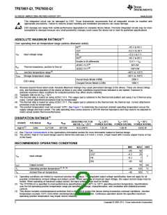
ABSOLUTE MAXIMUM RATINGS(1)
Over operating free-air temperature range (unless otherwise noted).
IN(2)
–65 V to 60 V
–0.3 V to 28 V
–0.3 V to 7 V
–65 V to 60 V
0.6 V < VIN
60°C/W
OUT
VIN
Input voltage range
FB
EN(2)
Enable to IN differential
JEDEC 51-5(3)
JEDEC 51-7(4)
θJA
Thermal impedance, junction to free air
130°C/W
TJ
Junction temperature range(5)
Storage temperature range
–40°C to 125°C
–65°C to 150°C
2000 V
TSTG
Human-Body Model (HBM)
ESD rating
Charged-Device Model (CDM)
1000 V
(1) Stresses beyond those listed under Absolute Maximum Ratings may cause permanent damage to the device. These are stress ratings
only, and functional operation of the device at these or any other conditions beyond those indicated is not implied. Exposure to
absolute-maximum-rated conditions for extended periods may affect device reliability.
(2) Transient: 500 ms for VIN > 50 V
(3) The thermal data is based on using JEDEC 51-5. The copper pad is soldered to the thermal land pattern and using 5 by 8 thermal array
(vias). Correct attachment procedure must be incorporated.
(4) The thermal data is based on using JEDEC 51-7. The copper pad is soldered to the thermal land. No thermal vias. Correct attachment
procedure must be incorporated.
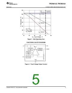
(5) The junction temperature must not exceed 125ºC. See Figure 1 to determine the maximum ambient operating temperature versus the
supply voltage and load current. The safe operating area curves assume a 50ºC/W thermal impedance and may need to be adjusted to
match actual system thermal performance.
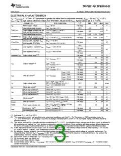
DISSIPATION RATINGS(1)
DERATING FACTOR
ABOVE TA = 25°C
T
A ≤ 25°C
TA = 70°C
TA = 85°C
BOARD
PACKAGE
RθJC
RθJA
POWER RATING POWER RATING POWER RATING
High-K(2)
DGN
8.2°C/W
60°C/W
16.6 mW/°C
1.83 W 1.08 W 0.833 W
(1) See Thermal Considerations in the Applications Information section for more information related to thermal design.
(2) The JEDEC High-K (1s) board design used to derive this data was a 4.5-inch x 3-inch, 2-layer board with 2-ounce copper traces on top
of the board.
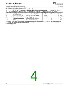
RECOMMENDED OPERATING CONDITIONS
MIN
–65
MAX UNIT
IN
50
OUT
FB
–0.3
–0.3
–65
28
V
VIN
Input voltage
7
EN
50
IOUT
TJ
Output current
Operating junction temperature(1) (2) (3)
50
125
105
mA
°C
–40
–40
TA
Ambient free-air temperature
°C
(1) Operating conditions are limited by maximum junction temperature. The regulated output voltage specification does not apply for all
possible combinations of input voltage and output current. When operating at maximum input voltage, the output current range must be
limited. When operating at maximum output current, the input voltage range must be limited.
(2) The TPS798xxQ is specified to meet performance specifications from –40°C to 125°C operating junction temperature. Specifications
over the full operating junction temperature range are specified by design, characterization, and correlation with statistical process
controls.
(3) This device includes overtemperature protection that is intended to protect the device during momentary overload conditions. Junction
temperature exceeds 125°C (min) when overtemperature protection is active. Continuous operation above the specified maximum
operating junction temperature may impair device reliability.
2
Copyright © 2009–2011, Texas Instruments Incorporated

 TI [ TEXAS INSTRUMENTS ]