TPS732xx
www.ti.com
SBVS037I–AUGUST 2003–REVISED MAY 2006
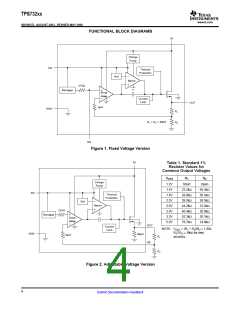
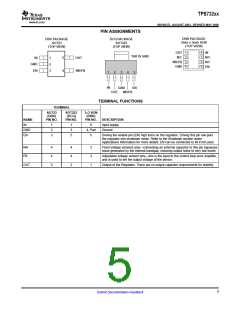
PIN ASSIGNMENTS
DRB PACKAGE
3mm x 3mm SON
(TOP VIEW)
DBV PACKAGE
SOT23
(TOP VIEW)
DCQ PACKAGE
SOT223
(TOP VIEW)
OUT
N/C
1
2
3
4
8
7
6
5
IN
TAB IS GND
N/C
N/C
EN
5
4
IN
GND
EN
1
2
3
OUT
NR/FB
GND
NR/FB
1
2
3
4
5
IN
GND
EN
OUT
NR/FB
TERMINAL FUNCTIONS
TERMINAL
SOT23
(DBV)
SOT223
(DCQ)
3×3 SON
(DRB)
NAME
PIN NO.
PIN NO.
PIN NO.
DESCRIPTION
Input supply
Ground
IN
1
2
3
1
3
5
8
4, Pad
5
GND
EN
Driving the enable pin (EN) high turns on the regulator. Driving this pin low puts
the regulator into shutdown mode. Refer to the Shutdown section under
Applications Information for more details. EN can be connected to IN if not used.
NR
4
4
5
4
4
2
3
3
1
Fixed voltage versions only—connecting an external capacitor to this pin bypasses
noise generated by the internal bandgap, reducing output noise to very low levels.
FB
Adjustable voltage version only—this is the input to the control loop error amplifier,
and is used to set the output voltage of the device.
OUT
Output of the Regulator. There are no output capacitor requirements for stability.
5
Submit Documentation Feedback

 TI [ TEXAS INSTRUMENTS ]