TPS65910, TPS65910A, TPS65910A3, TPS659101, TPS659102, TPS659103
TPS659104, TPS659105, TPS659106, TPS659107, TPS659108, TPS659109
www.ti.com
SWCS046N –MARCH 2010–REVISED APRIL 2012
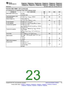
VDAC AND VPLL LDO (continued)
over operating free-air temperature range (unless otherwise noted)
PARAMETER
TEST CONDITIONS
VIN = 2.5 V, IOUT = IOUTmax, T = 25°C
On mode, IOUT = IOUTmax to 0
MIN
TYP
MAX
UNIT
DC load regulation
10
1
mV
mV
DC line regulation
On mode, VIN = VINmin to VINmax @ IOUT = IOUTmax
On mode, VIN = 3.8 V, IOUT = 0.1 × IOUTmax to 0.9 ×
IOUTmax in 5 µs
Transient load regulation
9
mV
And IOUT = 0.9 × IOUTmax to 0.1 × IOUTmax in 5 µs
On mode, VIN = VINmin + 0.5 V to VINmin in 30 µs
Transient line regulation
0.5
mV
And VIN = VINmin to VINmin + 0.5 V in 30 µs, IOUT
IOUTmax/2
=
Turn-on time
IOUT = 0, @ VOUT = 0.1 V up to VOUTmin
100
300
µs
Turn-on inrush current
mA
VIN = VINDC + 100 mVpp tone, VINDC+ = 3.8 V, IOUT
IOUTmax/2
=
Ripple rejection
f = 217 Hz
70
40
dB
f = 50 kHz
VPLL internal resistance
Ground current
LDO off
535
60
kΩ
On mode, IOUT = 0
On mode, IOUT = IOUTmax
Low-power mode
Off mode
1600
12
µA
1
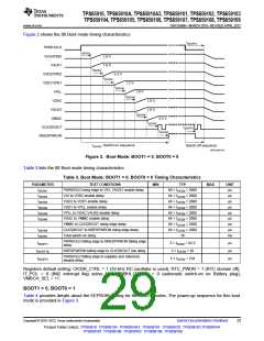
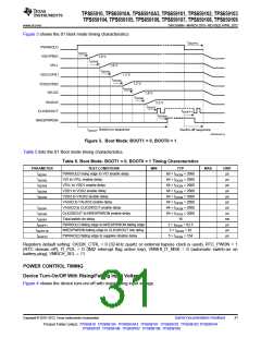
SWITCH-ON/-OFF SEQUENCES AND TIMING
Time slot length can be selected to be 0.5 ms or 2 ms through the EEPROM for an OFF-to-ACTIVE transition or
through the value programmed in the register DEVCTRL2_REG for a SLEEP-to-ACTIVE transition.
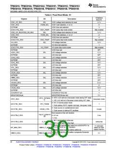
BOOT1 = 0, BOOT0 = 0
Table 2 provides details about the EEPROM setting for the BOOT modes. The power-up sequence for this boot
mode is provided in Figure 2.
Table 2. Fixed Boot Mode: 00
TPS65910
Boot 00
Register
VDD1_OP_REG
Bit
Description
SEL
VDD1 voltage level selection for boot
VDD1 Gain selection, x1 or x2
VDD1 time slot selection
VDD1 pulse skip mode enable
VDD2 voltage level selection for boot
VDD2 Gain selection, x1 or x3
VDD2 time slot selection
VDD2 pulse skip mode enable
VIO voltage selection
1.2 V
VDD1_REG
VGAIN_SEL
x1
EEPROM
3
skip enabled
1.1 V
DCDCCTRL_REG
VDD2_OP_REG/VDD2_SR_REG
VDD2_REG
VDD1_PSKIP
SEL
VGAIN_SEL
x3
EEPROM
2
DCDCCTRL_REG
VIO_REG
VDD2_PSKIP
SEL
skip enabled
1.8 V
EEPROM
VIO time slot selection
1
DCDCCTRL_REG
EEPROM
VIO_PSKIP
SEL
VIO pulse skip mode enable
VDD3 time slot
skip enabled
OFF
VDIG1_REG
EEPROM
LDO voltage selection
1.2 V
LDO time slot
OFF
VDIG2_REG
SEL
LDO voltage selection
1.0 V
Copyright © 2010–2012, Texas Instruments Incorporated
Submit Documentation Feedback
27
Product Folder Link(s): TPS65910 TPS65910A TPS65910A3 TPS659101 TPS659102 TPS659103 TPS659104
TPS659105 TPS659106 TPS659107 TPS659108 TPS659109

 TI [ TEXAS INSTRUMENTS ]