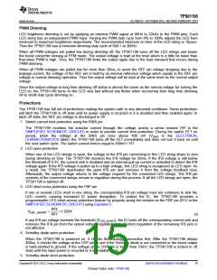
TPS61196
www.ti.com
SLVSBG1C –OCTOBER 2012–REVISED FEBRUARY 2013
DETAILED DESCRIPTION
Supply Voltage
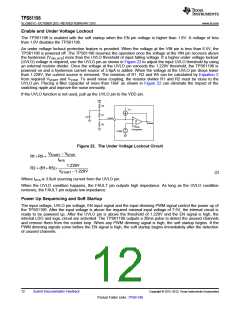
The TPS61196 has a built-in linear regulator to supply the IC analog and logic circuitry. The VDD pin, output of
the regulator, must be connected to a 1.0µF bypass capacitor. VDD only has a current sourcing capability of
15mA. VDD voltage is ready after the EN pin is pulled high.
Boost Controller
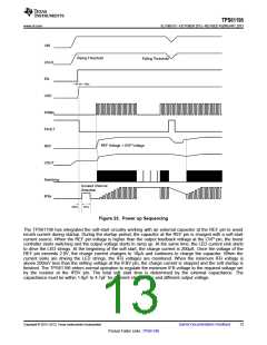
The TPS61196 regulates the output voltage with current mode PWM (pulse width modulation) control. The
control circuitry turns on an external switch FET at the beginning of each switching cycle. The input voltage is
applied across the inductor and stores the energy as the inductor current ramps up. During this portion of the
switching cycle, the load current is provided by the output capacitor. When the inductor current rises to the
threshold set by the Error Amplifier (EA) output, the switch FET is turned off and the external Schottky diode is
forward biased. The inductor transfers stored energy to replenish the output capacitor and supply the load
current. This operation repeats each switching cycle. The switching frequency is programmed by an external
resistor.
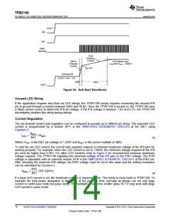
A ramp signal from the oscillator is added to the current ramp to provide slope compensation, shown in the
Functional Block Diagram. The duty cycle of the converter is then determined by the PWM Logic block which
compares the EA output and the slope compensated current ramp. The feedback loop regulates the OVP pin to
a reference voltage generated by the minimum voltage across the IFB pins. The output of the EA is connected to
the COMP pin. An external RC compensation network must be connected to the COMP pin to optimize the
feedback loop for stability and transient response.
The TPS61196 consistently adjusts the boost output voltage to account for any changes in LED forward
voltages. In the event that the boost controller is not able to regulate the output voltage due to the minimum
pulse width (ton(min), in the ELECTRICAL CHARACTERISTICS table), the TPS61196 enters pulse skip mode. In
this mode, the device keeps the power switch off for several switching cycles to prevent the output voltage from
rising above the regulated voltage. This operation typically occurs in light load condition or when the input voltage
is higher than the output voltage.
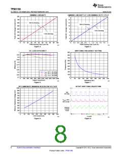
Switching Frequency
The switching frequency is programmed between 100kHz to 800kHz by an external resistor (R9 in the
SIMPLIFIED SCHEMATIC CIRCUIT). To determine the resistance by a given frequency, use the curve in
Figure 7 or calculate the resistance value by Equation 1. Table 2 shows the recommended resistance values for
some switching frequencies.
40000
fSW
=
kHz
( )
R9
(1)
Table 2. Recommended Resistance Values for
Switching Frequencies
R9
fSW
400 k
200 k
100 k
80 k
100 kHz
200 kHz
400 kHz
500 kHz
800 kHz
48 k
Copyright © 2012–2013, Texas Instruments Incorporated
Submit Documentation Feedback
11
Product Folder Links :TPS61196

 TI [ TEXAS INSTRUMENTS ]