TPS54560
SLVSBN0 –MARCH 2013
www.ti.com
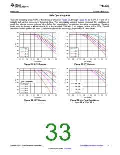
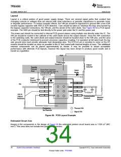
Layout
Layout is a critical portion of good power supply design. There are several signal paths that conduct fast
changing currents or voltages that can interact with stray inductance or parasitic capacitance to generate noise
or degrade performance. To reduce parasitic effects, the VIN pin should be bypassed to ground with a low ESR
ceramic bypass capacitor with X5R or X7R dielectric. Care should be taken to minimize the loop area formed by
the bypass capacitor connections, the VIN pin, and the anode of the catch diode. See Figure 60 for a PCB layout
example. The GND pin should be tied directly to the power pad under the IC and the power pad.
The power pad should be connected to internal PCB ground planes using multiple vias directly under the IC. The
SW pin should be routed to the cathode of the catch diode and to the output inductor. Since the SW connection
is the switching node, the catch diode and output inductor should be located close to the SW pins, and the area
of the PCB conductor minimized to prevent excessive capacitive coupling. For operation at full rated load, the top
side ground area must provide adequate heat dissipating area. The RT/CLK pin is sensitive to noise so the RT
resistor should be located as close as possible to the IC and routed with minimal lengths of trace. The additional
external components can be placed approximately as shown. It may be possible to obtain acceptable
performance with alternate PCB layouts, however this layout has been shown to produce good results and is
meant as a guideline.
Vout
Output
Capacitor
Output
Inductor
Topside
Ground
Route Boot Capacitor
Catch
Area
Trace on another layer to
provide wide path for
topside ground
Diode
Input
Bypass
Capacitor
BOOT
VIN
SW
GND
COMP
FB
Vin
EN
UVLO
RT/CLK
Compensation
Network
Adjust
Resistor
Divider
Resistors
Frequency
Thermal VIA
Signal VIA
Set Resistor
Figure 60. PCB Layout Example
Estimated Circuit Area
Boxing in the components in the design of Figure 35 the estimated printed circuit board area is 1.025 in2 (661
mm2). This area does not include test points or connectors.
34
Submit Documentation Feedback
Copyright © 2013, Texas Instruments Incorporated
Product Folder Links: TPS54560

 TI [ TEXAS INSTRUMENTS ]