TPS54540
SLVSBX7 –MAY 2013
www.ti.com
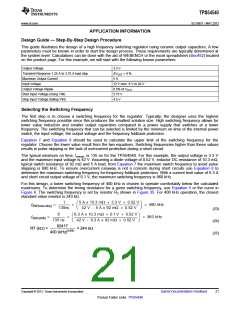
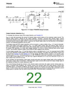
L1
5.5uH
VOUT
0.1uF
C4
3.3V, 5A
C6
C7
U1
TPS54540DDA
D1
100uF 100uF
PDS760
8
7
6
5
1
2
3
4
R5
31.6k
BOOT
SW
GND
COMP
FB
VIN
6V to 42V
C1
VIN
EN
C10
C3
C2
4.7uF
R1
365k
FB
FB
RT/CLK
4.7uF
4.7uF
4.7uF
R4
16.9k
9
C8
47pF
R6
10.2k
R2
88.7k
R3
243k
C5
4700pF
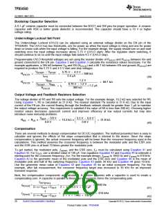
Figure 35. 5 V Output TPS54540 Design Example.
Output Inductor Selection (LO)
To calculate the minimum value of the output inductor, use Equation 26.
KIND is a ratio that represents the amount of inductor ripple current relative to the maximum output current. The
inductor ripple current is filtered by the output capacitor. Therefore, choosing high inductor ripple currents
impacts the selection of the output capacitor since the output capacitor must have a ripple current rating equal to
or greater than the inductor ripple current. In general, the inductor ripple value is at the discretion of the designer,
however, the following guidelines may be used.
For designs using low ESR output capacitors such as ceramics, a value as high as KIND = 0.3 may be desirable.
When using higher ESR output capacitors, KIND = 0.2 yields better results. Since the inductor ripple current is
part of the current mode PWM control system, the inductor ripple current should always be greater than 150 mA
for stable PWM operation. In a wide input voltage regulator, it is best to choose relatively large inductor ripple
current. This provides sufficienct ripple current with the input voltage at the minimum.
For this design example, KIND = 0.3 and the inductor value is calculated to be 5.1 μH. It is important that the RMS
current and saturation current ratings of the inductor not be exceeded. The RMS and peak inductor current can
be found from Equation 28 and Equation 29. For this design, the RMS inductor current is 5 A and the peak
inductor current is 5.79 A. The chosen inductor is a WE 744325550, which has a saturation current rating of 12 A
and an RMS current rating of 10 A. This also has a typical inductance of 5.5 µH at no load and 4.8 µH at 5 A
load. Lastly it has a DCR of 10.3 mΩ.
As the equation set demonstrates, lower ripple currents will reduce the output voltage ripple of the regulator but
will require a larger value of inductance. Selecting higher ripple currents will increase the output voltage ripple of
the regulator but allow for a lower inductance value.
The current flowing through the inductor is the inductor ripple current plus the output current. During power up,
faults or transient load conditions, the inductor current can increase above the peak inductor current level
calculated above. In transient conditions, the inductor current can increase up to the switch current limit of the
device. For this reason, the most conservative design approach is to choose an inductor with a saturation current
rating equal to or greater than the switch current limit of the TPS54540 which is nominally 7.5 A.
22
Submit Documentation Feedback
Copyright © 2013, Texas Instruments Incorporated
Product Folder Links: TPS54540

 TI [ TEXAS INSTRUMENTS ]