TPS54540
www.ti.com
SLVSBX7 –MAY 2013
APPLICATION INFORMATION
Design Guide — Step-By-Step Design Procedure
This guide illustrates the design of a high frequency switching regulator using ceramic output capacitors. A few
parameters must be known in order to start the design process. These requirements are typically determined at
the system level. Calculations can be done with the aid of WEBENCH or the excel spreadsheet (slvc452) located
on the product page. For this example, we will start with the following known parameters:
Output Voltage
3.3 V
Transient Response 1.25 A to 3.75 A load step
Maximum Output Current
Input Voltage
ΔVOUT = 4 %
5 A
12 V nom. 6 V to 42 V
0.5% of VOUT
5.75 V
Output Voltage Ripple
Start Input Voltage (rising VIN)
Stop Input Voltage (falling VIN)
4.5 V
Selecting the Switching Frequency
The first step is to choose a switching frequency for the regulator. Typically, the designer uses the highest
switching frequency possible since this produces the smallest solution size. High switching frequency allows for
lower value inductors and smaller output capacitors compared to a power supply that switches at a lower
frequency. The switching frequency that can be selected is limited by the minimum on-time of the internal power
switch, the input voltage, the output voltage and the frequency foldback protection.
Equation 7 and Equation 8 should be used to calculate the upper limit of the switching frequency for the
regulator. Choose the lower value result from the two equations. Switching frequencies higher than these values
results in pulse skipping or the lack of overcurrent protection during a short circuit.
The typical minimum on time, tonmin, is 135 ns for the TPS54540. For this example, the output voltage is 3.3 V
and the maximum input voltage is 42 V. Assuming a diode voltage of 0.52 V, inductor DC resistance of 10.3 mΩ,
typical switch resistance of 92 mΩ and 5 A load, from Equation 7 the maximum switch frequency to avoid pulse
skipping is 680 kHz. To ensure overcurrent runaway is not a concern during short circuits use Equation 8 to
determine the maximum switching frequency for frequency foldback protection. With a current limit value of 6.3 A
and short circuit output voltage of 0.1 V, the maximum switching frequency is 960 kHz.
For this design, a lower switching frequency of 400 kHz is chosen to operate comfortably below the calculated
maximums. To determine the timing resistance for a given switching frequency, use Equation 5 or the curve in
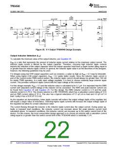
Figure 6. The switching frequency is set by resistor R3 shown in Figure 35. For 400 kHz operation, the closest
standard value resistor is 243 kΩ.
1
5 A x 10.3 mW + 3.3 V + 0.52 V
42 V - 5 A x 92 mW + 0.52 V
æ
ö
fSW(maxskip)
=
´
= 680 kHz
ç
÷
135ns
è
ø
(23)
(24)
(25)
8
6.3 A x 10.3 mW + 0.1 V + 0.52 V
42 V - 6.3 A x 92 mW + 0.52 V
æ
ö
fSW(shift)
=
´
= 960 kHz
ç
÷
135 ns
è
ø
92417
400 (kHz)0.991
RT (kW) =
= 244 kW
Copyright © 2013, Texas Instruments Incorporated
Submit Documentation Feedback
21
Product Folder Links: TPS54540

 TI [ TEXAS INSTRUMENTS ]