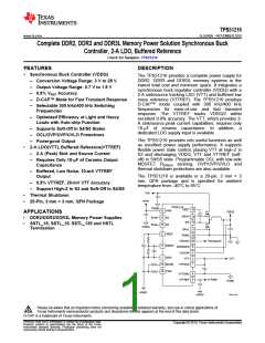
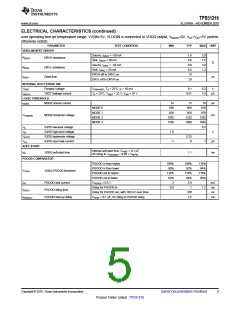
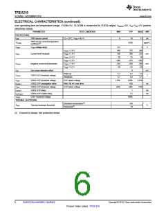
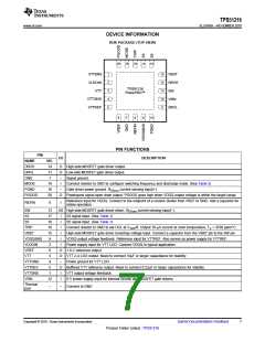
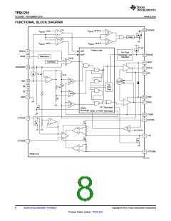
TPS51216
SLUSAB9 –NOVEMBER 2010
www.ti.com
These devices have limited built-in ESD protection. The leads should be shorted together or the device placed in conductive foam
during storage or handling to prevent electrostatic damage to the MOS gates.
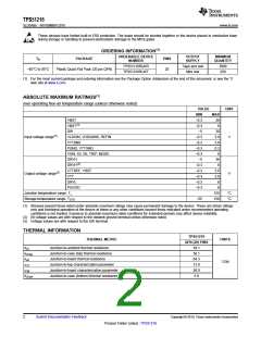
ORDERING INFORMATION(1)
ORDERABLE DEVICE
NUMBER
OUTPUT
SUPPLY
MINIMUM
QUANTITY
TA
PACKAGE
PINS
TPS51216RUKR
TPS51216RUKT
Tape and reel
Mini reel
3000
250
–40°C to 85°C
Plastic Quad Flat Pack (20 pin QFN)
20
(1) For the most current package and ordering information see the Package Option Addendum at the end of this document, or see the TI
web site at www.ti.com.
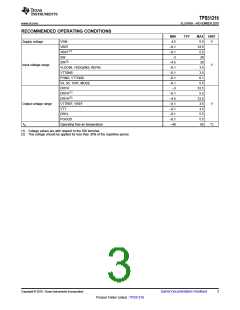
ABSOLUTE MAXIMUM RATINGS(1)
over operating free-air temperature range (unless otherwise noted)
VALUE
MIN
UNIT
MAX
36
6
VBST
VBST(3)
–0.3
–0.3
–5
SW
30
3.6
3.6
0.3
6
Input voltage range(2)
VLDOIN, VDDQSNS, REFIN
VTTSNS
–0.3
–0.3
–0.3
–0.3
–5
V
PGND, VTTGND
V5IN, S3, S5, TRIP, MODE
DRVH
36
6
DRVH(3)
–0.3
–0.3
–0.3
–0.3
–0.3
VTTREF, VREF
VTT
3.6
3.6
6
Output voltage range(2)
V
DRVL
PGOOD
6
Junction temperature range, TJ
Storage temperature range, TSTG
125
150
°C
°C
–55
(1) Stresses beyond those listed under absolute maximum ratings may cause permanent damage to the device. These are stress ratings
only and functional operation of the device at these or any other conditions beyond those indicated under recommended operating
conditions is not implied. Exposure to absolute-maximum-rated conditions for extended periods may affect device reliability.
(2) All voltage values are with respect to the network ground terminal unless otherwise noted.
(3) Voltage values are with respect to the SW terminal.
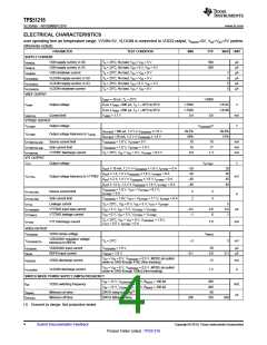
THERMAL INFORMATION
TPS51216
THERMAL METRIC
UNITS
QFN (20) PINS
qJA
Junction-to-ambient thermal resistance
94.1
58.1
64.3
31.8
58.0
5.9
qJCtop
qJB
Junction-to-case (top) thermal resistance
Junction-to-board thermal resistance
°C/W
yJT
Junction-to-top characterization parameter
Junction-to-board characterization parameter
Junction-to-case (bottom) thermal resistance
yJB
qJCbot
2
Submit Documentation Feedback
Copyright © 2010, Texas Instruments Incorporated
Product Folder Link(s) :TPS51216

 TI [ TEXAS INSTRUMENTS ]