TPS51216
www.ti.com
SLUSAB9 –NOVEMBER 2010
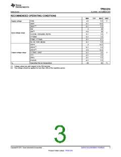
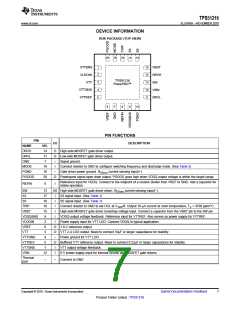
DEVICE INFORMATION
RUK PACKAGE (TOP VIEW)
20
19
18
17
16
1
2
3
4
5
15
14
13
12
11
VTTSNS
VLDOIN
VTT
VBST
DRVH
SW
TPS51216
PowerPAD™
VTTGND
VTTREF
V5IN
DRVL
6
7
8
9
10
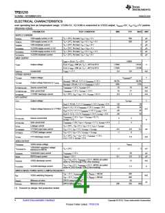
PIN FUNCTIONS
PIN
NAME
DRVH
I/O
DESCRIPTION
NO.
14
11
7
O
O
–
High-side MOSFET gate driver output.
Low-side MOSFET gate driver output.
Signal ground.
DRVL
GND
MODE
PGND
19
10
20
I
Connect resistor to GND to configure switching frequency and discharge mode. (See Table 2)
Gate driver power ground. RDS(on) current sensing input(+).
–
PGOOD
O
Powergood signal open drain output. PGOOD goes high when VDDQ output voltage is within the target range.
Reference input for VDDQ. Connect to the midpoint of a resistor divider from VREF to GND. Add a capacitor for
stable operation.
REFIN
8
I
SW
13
17
16
18
15
9
I/O High-side MOSFET gate driver return. RDS(on) current sensing input(–).
S3
I
I
S3 signal input. (See Table 1)
S5
S5 signal input. (See Table 1)
TRIP
I
Connect resistor to GND to set OCL at VTRIP/8. Output 10-mA current at room temperature, TC = 4700 ppm/°C.
High-side MOSFET gate driver bootstrap voltage input. Connect a capacitor from the VBST pin to the SW pin.
VDDQ output voltage feedback. Reference input for VTTREF. Also serves as power supply for VTTREF.
Power supply input for VTT LDO. Connect VDDQ in typical application.
1.8-V reference output.
VBST
VDDQSNS
VLDOIN
VREF
VTT
I
I
2
I
6
O
O
–
O
I
3
VTT 2-A LDO output. Need to connect 10mF or larger capacitance for stability.
Power ground for VTT LDO.
VTTGND
VTTREF
VTTSNS
V5IN
4
5
Buffered VTT reference output. Need to connect 0.22mF or larger capacitance for stability.
VTT output voltage feedback.
1
12
I
5-V power supply input for internal circuits and MOSFET gate drivers.
Thermal
pad
–
–
Connect to GND
Copyright © 2010, Texas Instruments Incorporated
Submit Documentation Feedback
7
Product Folder Link(s) :TPS51216

 TI [ TEXAS INSTRUMENTS ]