TPS40200-Q1
SLUS739D –SEPTEMBER 2006–REVISED JULY 2011
www.ti.com
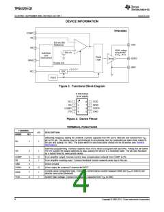
DEVICE INFORMATION
TPS40200
COMP 3
FB 4
–
E/A and SS
Reference
VDD
8
SS
2
+
GDRV voltage
swing limited
to (VIN – 8 V)
700 mV
+
Soft-Start
and
Overcurrent
PWM
Logic
6
5
Driver
GDRV
GND
ISNS
RC
7
1
Enable E/A
OSC
UVLO
Figure 3. Functional Block Diagram
D PACKAGE
(TOP VIEW)
RC
SS
VDD
1
2
3
4
8
7
6
5
ISNS
GDRV
GND
COMP
FB
Figure 4. Device Pinout
TERMINAL FUNCTIONS
TERMINAL
I/O
DESCRIPTION
NAME
NO.
Switching frequency setting RC network. Connect capacitor from RC pin to GND pin and resistor from VIN
pin to RC pin. The device may be synchronized to an external clock by connecting an open-drain output to
this pin and pulling it to GND. The pulse width for synchronization should not be excessive (see General
Information).
RC
1
I
Soft-start programming. Connect capacitor from SS to GND to program soft start time. Pulling this pin below
150 mV causes the output switching to stop, placing the device in a shutdown state. The pin also functions
as a restart timer for overcurrent events.
SS
2
I
COMP
FB
3
4
5
6
O
I
Error amplifier output. Connect control loop compensation network from COMP to FB.
Error amplifier inverting input. Connect feedback resistor network center tap to this pin.
Device ground
GND
GDRV
O
I
Driver output for external P-channel MOSFET
Current-sense comparator input. Connect a current sense resistor between ISNS and VDD in order to set
desired overcurrent threshold.
ISNS
VDD
7
8
I
System input voltage. Connect local bypass capacitor from VDD to GND.
4
Copyright © 2006–2011, Texas Instruments Incorporated

 TI [ TEXAS INSTRUMENTS ]