TPS40200-Q1
www.ti.com
SLUS739D –SEPTEMBER 2006–REVISED JULY 2011
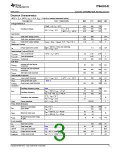
Electrical Characteristics
–40°C < TA < 125°C, VDD = 12 V, fOSC = 100 kHz (unless otherwise noted)
PARAMETER
Voltage Reference
TEST CONDITIONS
MIN
TYP
MAX
UNIT
COMP = FB, TA = 25°C
689
686
676
696
696
696
702
703
712
VFB
Feedback voltage
TA = 25°C
mV
4.5 V < VDD < 52 V
–40°C < TA < 125°C
Gate Driver
Isrc
Gate driver pullup current
Gate driver pulldown current
Gate driver output voltage
125
200
5.6
300
300
8
mA
mA
V
Isnk
VGATE
VGATE = (VDD – VGDRV), 12 V < VDD < 52 V
10
Quiescent Current
fOSC = 300 kHz, Driver not switching,
4.5 V < VDD < 52 V
Iqq
Device quiescent current
1.5
3.0
mA
Undervoltage Lockout (UVLO)
VUVLO(on)
VUVLO(off)
Turn-on threshold
Turn-off threshold
–40°C < TA < 125°C
3.8
4.25
4.05
200
4.55
275
V
V
VUVLO(HYST) Hysteresis
110
mV
Soft Start
Internal soft-start pullup
resistance
RSS(chg)
65
105
170
kΩ
Internal soft-start pulldown
resistance
RSS(dchg)
VSSRST
190
100
305
150
485
200
kΩ
Soft-start reset threshold
mV
Overcurrent Protection
VILIM
Overcurrent threshold
4.5 V < VDD < 52 V
–40°C < TA < 125°C
50
100
150
140
2
mV
%
OCDF
Overcurrent duty cycle
Note 1
VILIM(rst)
Oscillator
Overcurrent reset threshold
100
200
mV
Oscillator frequency range
Oscillator frequency
Note
35
85
500
118
345
0
fOSC
RRC = 200 kΩ, CRC = 470 pF
RRC = 68.1 kΩ, CRC = 470 pF
12 V < VDD < 52 V
100
300
kHz
210
-9
Frequency line regulation
Ramp amplitude
%
V
4.5 V < VDD < 12 V
–21
0
VRMP
4.5 V < VDD < 52 V
VDD/10
Pulse-Width Modulator
VDD = 12 V
200
100
95
540
200
Minimum controllable
pulse width
tMIN
ns
VDD = 30 V
Fosc = 100 kHz, CL = 470 pF
Fosc = 300 kHz, CL = 470 pF
93
90
DMAX
KPWM
Maximum duty cycle
%
93
Modulator and power-stage
dc gain
8
10
12
V/V
Error Amplifier
IIB
Input bias current
100
80
250
nA
dB
AOL
Open loop gain
Note
60
1.5
100
1.0
GBWP
ICOMP(src)
ICOMP(snk)
Unity gain bandwidth
Output source current
Output sink current
Note
3
MHz
μA
VFB = 0.6 V, COMP = 1 V
VFB = 1.2 V, COMP = 1 V
250
2.5
mA
Copyright © 2006–2011, Texas Instruments Incorporated
3

 TI [ TEXAS INSTRUMENTS ]