TPS2149
TPS2159
SLVS401 – AUGUST 2001
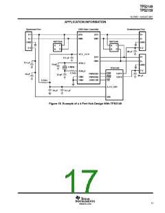
APPLICATION INFORMATION
overcurrent (continued)
In the second condition, the short occurs while the device is enabled. At the instant the short occurs, very high
currents may flow for a very short time before the current-limit circuit can react. After the current-limit circuit has
tripped (reached the overcurrent trip threshold), the device switches into constant-current mode.
In the third condition, the load has been gradually increased beyond the recommended operating current. The
current is permitted to rise until the current-limit threshold is reached or until the thermal limit of the device is
exceeded. TheTPS2149andTPS2159arecapableofdeliveringcurrentuptothecurrent-limitthresholdwithout
damagingthedevice. Oncethethresholdhasbeenreached, thedeviceswitchesintoitsconstant-currentmode.
OC response
The OC open-drain output is asserted (active low) when an overcurrent condition is encountered. The output
will remain asserted until the overcurrent condition is removed. Connecting a heavy capacitive load to an
enabled device can cause momentary false overcurrent reporting from the inrush current flowing through the
device, charging the downstream capacitor. The TPS2149 and TPS2159 are designed to reduce false
overcurrent reporting. An internal overcurrent transient filter eliminates the need for external components to
removeunwantedpulses. Usinglow-ESRelectrolyticcapacitorsonOUTxlowerstheinrushcurrentflowthrough
the device during hot-plug events by providing a low-impedance energy source, also reducing erroneous
overcurrent reporting.
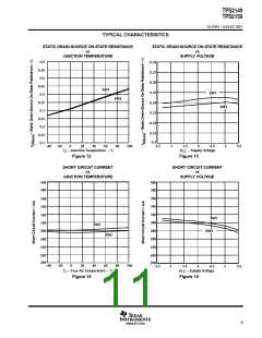
power dissipation and junction temperature
The main source of power dissipation for the TPS2149 and TPS2159 comes from the internal voltage regulator
and the N-channel MOSFETs. Checking the power dissipation and junction temperature is always a good
designpracticeanditstartswithdeterminingther
oftheN-channelMOSFETaccordingtotheinputvoltage
(on)
DS
and operating temperature. As an initial estimate, use the highest operating ambient temperature of interest and
read r from the graphs shown in the Typical Characteristics section of this data sheet. Using this value,
(on)
DS
the power dissipation per switch can be calculated using:
2
P
r
I
D
DS(on)
(1)
(2)
Multiply this number by two to get the total power dissipation coming from the N-channel MOSFETs.
The power dissipation for the internal voltage regulator is calculated using:
P
V –V
I
D
I
O(min)
O
The total power dissipation for the device becomes:
P
P
2
P
D(total)
D(voltage regulator)
Finally, calculate the junction temperature:
D(switch)
(3)
(4)
T
P
R
T
J
D
JA
A
Where:
T = Ambient temperature °C
A
R
= Thermal resistance °C/W, equal to inverting the derating factor found on the power dissipation
θJA
table in this datasheet.
13
www.ti.com

 TI [ TEXAS INSTRUMENTS ]