TPS20xxC
SLVSAU6A –JUNE 2011–REVISED JULY 2011
www.ti.com
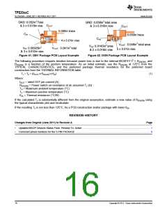
GND: 0.052in2 Total
GND: 0.056in2 total area
& 3 x 0.018in vias
COUT
& 3 x 0.018in vias
COUT
0.050in trace
CIN
0.050in trace
CIN
4 x 0.01in vias
VOUT: 0.048in2 total area
5 x 0.01in vias
VIN: 0.0145in2 area
& 2 x 0.018in vias
V : 0.00925in2
VOUT: 0.041in2 total
IN
& 3 x 0.018in vias
Figure 41. DBV Package PCB Layout Example
Figure 42. DGN Package PCB Layout Example
The following procedure requires iteration because power loss is due to the internal MOSFET I2 × RDS(ON), and
RDS(ON) is a function of the junction temperature. As an initial estimate, use the RDS(ON) at 125°C from the
TYPICAL CHARACTERISTICS, and the preferred package thermal resistance for the preferred board
construction from the THERMAL INFORMATION table.
TJ = TA + ((IOUT2 x RDS(ON)) x θJA)
(1)
Where:
IOUT = rated OUT pin current (A)
RDS(ON) = Power switch on-resistance at an assumed TJ (Ω)
TA = Maximum ambient temperature (°C)
TJ = Maximum junction temperature (°C)
θJA = Thermal resistance (°C/W)
If the calculated TJ is substantially different from the original assumption, estimate a new value of RDS(ON) using
the typical characteristic plot and recalculate.
If the resulting TJ is not less than 125°C, try a PCB construction and/or package with lower θJA
.
SPACER
REVISION HISTORY
Changes from Original (June 2011) to Revision A
Page
•
•
Updated MSOP Devices Status From: Preview To: Active .................................................................................................. 1
Corrected pinout numbers for the 5-PIN PACKAGE ............................................................................................................ 6
16
Copyright © 2011, Texas Instruments Incorporated

 TI [ TEXAS INSTRUMENTS ]