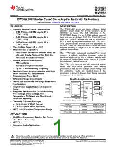
TPA3116D2
TPA3118D2
TPA3130D2
www.ti.com
SLOS708B –APRIL 2012–REVISED MAY 2012
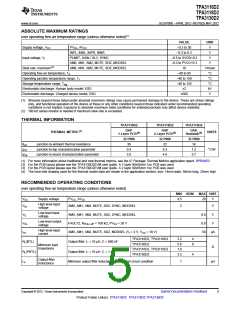
ABSOLUTE MAXIMUM RATINGS
over operating free-air temperature range (unless otherwise noted)(1)
VALUE
–0.3 to 30
–0.3 to 6.3
–0.3 to GVDD+0.3
–0.3 to PVCC+0.3
10
UNIT
Supply voltage, VCC
Input voltage, VI
PVCC, AVCC
V
V
INPL, INNL, INPR, INNR
PLIMIT, GAIN / SLV, SYNC
AM0, AM1, AM2, MUTE, SDZ, MODSEL
AM0, AM1, AM2, MUTE, SDZ, MODSEL
V
V
Slew rate, maximum(2)
V/msec
°C
Operating free-air temperature, TA
–40 to 85
–40 to 150
–40 to 125
±2
Operating junction temperature range, TJ
Storage temperature range, Tstg
°C
°C
Electrostatic discharge: Human body model, ESD
Electrostatic discharge: Charged device model, ESD
kV
V
±500
(1) Stresses beyond those listed under absolute maximum ratings may cause permanent damage to the device. These are stress ratings
only, and functional operation of the device at these or any other conditions beyond those indicated under recommended operating
conditions is not implied. Exposure to absolute-maximum-rated conditions for extended periods may affect device reliability.
(2) 100 kΩ series resistor is needed if maximum slew rate is exceeded.
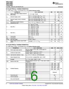
THERMAL INFORMATION
TPA3130D2
TPA3118D2
TPA3116D2
DAP
DAP
DAD
THERMAL METRIC(1)
UNITS
1 Layer PCB(2)
2 Layer PCB(3)
Heatsink(4)
32 PINS
36
32 PINS
22
32 PINS
14
θJA
ψJT
ψJB
Junction-to-ambient thermal resistance
Junction-to-top characterization parameter
Junction-to-board characterization parameter
0.4
0.3
1.2
°C/W
5.9
4.8
5.7
(1) For more information about traditional and new thermal metrics, see the IC Package Thermal Metrics application report, SPRA953.
(2) For the PCB layout please see the TPA3130D2EVM user guide. A 1 layer 90x85mm 1oc PCB was used
(3) For the PCB layout please see the TPA3130D2EVM user guide. A 2 layer 90x85mm 1oc PCB was used
(4) The heat sink drawing used for the thermal model data are shown in the application section, size: 14mm wide, 50mm long, 25mm high.
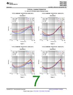
RECOMMENDED OPERATING CONDITIONS
over operating free-air temperature range (unless otherwise noted)
MIN NOM
MAX UNIT
VCC
VIH
Supply voltage
PVCC, AVCC
4.5
26
V
High-level input
voltage
AM0, AM1, AM2, MUTE, SDZ, SYNC, MODSEL
2
V
Low-level input
voltage
VIL
VOL
IIH
AM0, AM1, AM2, MUTE, SDZ, SYNC, MODSEL
FAULTZ, RPULL-UP = 100 kΩ, PVCC = 26 V
0.8
0.8
50
V
V
Low-level output
voltage
High-level input
current
AM0, AM1, AM2, MUTE, SDZ, MODSEL (VI = 2 V, VCC = 18 V)
µA
TPA3116D2, TPA3118D2
3.2
5.6
1.6
3.2
4
8
RL(BTL)
Output filter: L = 10 µH, C = 680 nF
Output filter: L = 10 µH, C = 1 µF
TPA3130D2
Minimum load
Impedance
Ω
TPA3116D2, TPA3118D2
TPA3130D2
RL(PBTL)
Lo
4
Output-filter
Inductance
Minimum output filter inductance under short-circuit condition
1
µH
Copyright © 2012, Texas Instruments Incorporated
Submit Documentation Feedback
5
Product Folder Link(s): TPA3116D2 TPA3118D2 TPA3130D2

 TI [ TEXAS INSTRUMENTS ]